LEVELs 49 and 53 BSIM3v3 MOS Models
The BSIM3v3 MOS model from UC Berkeley is available in Star-Hspice as LEVEL 49 and LEVEL 53. LEVEL 49 is an Hspice-enhanced version of BSIM3v3 while LEVEL 53 (first released in Star-Hspice 98.2) maintains full compliance with the Berkeley release. This compliance includes numerically identical model equations, identical parameter default values, and identical parameter range limits. LEVEL 49 maintains compliance with the UC Berkeley release of BSIM3v3 with the following three exceptions:
1.
Default parameter values.
Eliminate differences in default parameter values by explicit assignment of the parameters CAPMOD, XPART and by setting ACM=10.
2.
Parameter range limits.
Provides parameter range limits that are identical to that of the Berkeley release. Differences occur only in the severity of warning for five parameters. LEVEL 49 issues a warning that the parameter range has been exceeded but continues with simulation, whereas, in the Berkeley release, a fatal error is issued and simulation is aborted. These five parameters include NGATE, DVT1W, DVT1, DSUB, DROUT. (See the Model Parameter Range Limits below for more details.)
3.
Improvements in numerical stability.
Provides improvements in numerical stability. In most practical situations, these improvements will not affect compliance with the Berkeley release, but will improve convergence and simulation time.
Both LEVELs 49 and 53 support a superset of model parameters that include Hspice-specific parameters. For LEVEL 53, in all cases, Hspice-specific parameters default to OFF. The single exception in LEVEL 49 is that ACM defaults to 0. LEVEL 49 compliance with Berkeley BSIM3v3 can be achieved by setting ACM=10.
Selecting Model Versions
Recommended BSIM3v3 Version
As of the Star-Hspice 99.2 release (June 1999), the recommended BSIM3v3 model specification is LEVEL=49, VERSION=3.22. This version provides the most stable and up-to-date representation of the UCB BSIM3v3.2.2 model. However, do not change the VERSION specification in existing model cards without consulting the foundry or model extraction group that created the original model cards.
There are, as of the 99.2 release, five official BSIM3v3 releases from Berkeley and several Star-Hspice LEVEL 49 releases. (See the BSIM3 home page at http://www-device.EECS.Berkeley.EDU/~bsim3/ for additional release information from the UCB group.) To minimize confusion and maintain back compatibility, you can select the model parameters VERSION and HSPVER. VERSION selects the Berkeley release version and HSPVER selects the Star-Hspice release version. For example, HSPVER=97.2 and VERSION=3.1 reproduce results from Hspice 97.2 using the BSIM3 Version 3.1 model.
HSPVER defaults to the current release being executed. The model parameter, VERSION, selects among the various Berkeley releases of BSIM3v3 as follows:
-
Version 3.0 Berkeley release (October 30, 1995) default for HSPICE96.1,96.2,96.3. This version is invoked when VERSION=3.0 and HSPVER= 98.0 are specified. To invoke the Star-Hspice version that most accurately represents the Berkeley release of October 1995, specify the parameters VERSION=3.0 and HSPVER=98.0
-
Version 3.1 Berkeley (December 9, 1997) default for HSPICE97.1,97.2. 97.4. This version is invoked when VERSION=3.1 or 3.11 and HSPVER= 98.0 are specified. To invoke the Star-Hspice version that most accurately represents the Berkeley release of December, 1996 specify the parameters VERSION=3.1 or 3.11 and HSPVER = 98.0.
-
Berkeley Version 3.0, 3.1 bug fixes. Berkeley corrected several Version 3.0 and 3.1 bugs in the June, 1998 release. These bug fixes are incorporated into Hspice98.2 and are represented when VERSION=3.0 and VERSION=3.1 are specified respectively with HSPVER=98.2. As a result of bug fixes, some differences between Version 3.0/3.1 in Hspice98.2 and previous Version 3.0/3.1 releases are expected. Most notably, differences will occur when perimeter factors PD,PS less than Weff are specified (PD,PS < Weff are no longer clamped to Weff in Version 3.1) and when DLC and LINT are not identical (LeffCV calculation bug in Versions3.0, 3.1). You can find a complete list of bug fixes at the BSIM3 web site:
http://www-device.eecs.berkeley.edu/~bsim3.
NOTE: Version 3.11 was introduced in Hspice97.4. This version represented Berkeley Version 3.1 (Dec., 1996) with Hspice bug fixes. Back compatibility will be maintained for this model. Starting with Hspice98.2, Version 3.1 and 3.11 will be identical and represent Version 3.1 with Berkeley June, 1998 bug fixes.
-
Version 3.2 Berkeley release (June 16, 1998). This version is invoked when VERSION=3.2 and HSPVER=98.2 are specified.
-
Version 3.2.1 Berkeley release (April 20, 1999).
This version is invoked when VERSION=3.21 and HSPVER=99.2 are specified.
-
Version 3.2.2 Berkeley release (April 20, 1999).
This version is invoked when VERSION=3.22 and HSPVER=99.2 are specified.
NOTE: Versions 3.2.1 and 3.2.2 are identical except BSIM3v3.2.1 uses a bias-dependent Vfb and BSIM3v3.2.2 uses a bias-independent Vfb for the capacitance models capMod = 1 and 2.
The table below summarizes the Star-Hspice parameter settings required to match Berkeley releases:
|
Berkeley Release
|
VERSION
|
HSPVER
|
|
Version 3.0 (October 1995)
|
3.0
|
98.0
|
|
Version 3.0 with June 1998 bug fixes
|
3.0
|
98.2
|
|
Version 3.1 (December 1996)
|
3.1
|
98.0
|
|
Version 3.1 with June 1998 bug fixes
|
3.1
|
98.2
|
|
Version 3.2 (June 16,1998)
|
3.2
|
98.2
|
|
Version 3.2.1 (April 20, 1999)
|
3.21
|
99.2
|
|
Version 3.2.2 (April 20, 1999)
|
3.22
|
99.2
|
Version 3.2 Features
In June, 1998 Berkeley released BSIM3 Version 3.2, which contains many new features. These features are summarized below.
-
A new intrinsic capacitance model, CAPMOD=3, includes finite charge layer thickness effects; CAPMOD now defaults to 3 (new parameters: CAPMOD=3, ACDE, MOIN)
-
Improved modeling of C-V characteristics at the weak-to-strong inversion transition (new parameters: NOFF, VOFFCV)
-
Vth dependence on Tox (new parameter: TOXM)
-
Flatband voltage parameter more accurately models different gate materials (new parameter: VFB)
-
Improved substrate current scaleability with channel length, (new parameter: APLHA1)
-
Restructured nonquasi-static (NQS) model includes pole-zero analysis and bug fixes. Note that NQSMOD is now a BSIM3 element parameter. Hspice supports only the model parameter not the element parameter.
-
Junction diode model temperature dependence, (new parameters: TCJ, TCJSW, TCJSWG, TPB, TPBSW, TPBSWG)
-
Adjustable current limiting in the junction diode current model (new parameter: IJTH)
-
Option of using C-V inversion charge equations of CAPMOD=0,1,2,3 to calculate the thermal noise when NOIMOD=2 or 4
-
Elimination of small negative capacitance values (Cgs, Cgd) in the accumulation-depletion regions
-
A separate set of length/width dependence parameters for the CV model (New parameters: LLC, LWC, LWLC, WLC, WWC, WWLC)
-
Additional parameter checking
-
Bug fixes
NOTE: If all new Version 3.2 parameters are defaulted, Version 3.2 and Version 3.1 (with June, 1998 bug fixes) will give identical DC results. However, transient and AC results will differ, in general. This discrepancy arises only from differences in flatband voltage calculations used in the intrinsic charge/capacitance models. These differences occur in all CAPMOD models 1-3.
HSPVER < 98.0 will be reset to 98.0 for LEVEL 53.
HSPVER < 98.2 will be reset to 98.2 when VERSION >=3.2 for LEVELs 49 and 53.
Version 3.0, 3.1, and 3.11 in Hspice do not support NQSMOD and CAPMOD=3. These are supported only by Version 3.2.
You can obtain additional information about the Berkeley releases from the BSIM3 web site:
http://www-device.eecs.berkeley.edu/~bsim3.
Nonquasi-Static (NQS) Model
The Berkeley NonQuasi-Static (NQS) model is now available (as of the 98.2 release) in Star-Hspice for LEVELs 49 and 53. This model provides a first-order correction to the quasi-static charge models. See M.Chan, K.- Y. Hui, C. Hu, and P.-K. Ko, IEEE Trans. Electron Devices, vol. ED-45, pp.834-841, 1998. The Star-Hspice 98.2 release supports only the model parameter implementation.
To invoke the NQS model, specify the parameter NQSMOD=1 in the model card. NQSMOD can be used with any of the CAPMOD LEVELs (0-3) but is restricted to use with Version 3.2. NQS is not supported in Version 3.0 and 3.1. In future releases, the NQS will be supported in Versions 3.0, 3.1.
Star-Hspice Enhancements
Hspice Junction Diode Model and Area Calculation Method (ACM)
There are two junction diode models that can be used with both LEVELs 49 and 53: the Hspice junction model and the Berkeley junction model. The Hspice junction model is invoked by specifying the model parameter value ACM=0,1,2, or 3. The Berkeley junction model is invoked by specifying ACM=10,11,12, or 13. The default ACM value is 0 and 10 for LEVELs 49 and 53 respectively. The junction current, junction capacitance, and parasitic resistance equations corresponding to ACM=0,1,2,3 can be found in Selecting MOSFET Diode Models.
The effect of setting ACM=10,11,12, or 13 is to enable the Berkeley junction diodes and to add parasitic resistors to the MOSFET. The parasitic resistor equations for ACM=10-13 correspond to the ACM=0-3 parasitic resistor equations respectively. ACM=10-13 all use the Berkeley junction capacitance model equations:
(Bulk-source capacitance)
if (Ps > Weff)
Cbs = AS * Cjbs + (PS - Weff) * Cjbssw + Weff *
Cjbsswg
else
Cbs = AS * Cjbs + PS * Cjbsswg
Area and perimeter factors AS, PS default to 0 if not specified on the element line.
if (Vbs < 0)
Cjbs = Cj * (1 - (Vbs/Pb))-Mj
Cjbssw = Cjsw * (1 - (Vbs/Pbsw))-Mjsw
Cjbsswg = Cjswg * (1 - (Vbs/Pbswg))-Mjswg
else
Cjbs = Cj * (1 + Mj * (Vbs/Pb))
Cjbssw = Cjsw * (1 + Mjsw * (Vbs/Pbsw))
Cjbsswg = Cjswg * (1 + Mjswg * (Vbs/Pbswg))
Bulk-drain equations are analogous. Note that the Hspice equations for AS,PS,AD,PD are not used with ACM=10,11,12,13 and, in accordance with the BSIM3v3 model, the default values for these area and perimeter factors are zero. However, starting with Star-Hspice version 98.2, it is possible to invoke the Hspice calculations for AS,PS,AD,PD by specifying the model parameter CALCACM=1.
Important: CALCACM is only invoked when used with ACM=12.The calculations used in ACM=10, 11, 13 are not consistent with the Berkeley diode calculations.
With CALCACM = 1 and ACM = 12 the following area and perimeter calculations are invoked:
if AD is not specified on the element line:
AD = 2 * HDIFeff * Weff
else:
AD = AD * WMLT^2
if AS is not specified on the element line:
AS = 2 * HDIFeff * Weff
else:
AS = AS * WMLT^2
if PS is not specified on the element line:
PS = 4 * HDIFeff + 2 * Weff
else:
PS = PS * WMLT
if PD is not specified on the element line:
PD = 4 * HDIFeff + 2 * Weff
else:
PD = PD * WMLT
NOTE: Weff is not the same Weff used in the BSIM3v3, and LEVELs 49 and 53 I-V, C-V model equations!
In the preceding equations the following simple form is used.
Weff = W * WMLT + XW
where:
HDIFeff = HDIF * WMLT
|
W
|
is the width specified on the element line
|
|
HDIF
|
is a heavy diffusion length specified in the model card
|
|
WMLT
|
is a shrink factor specified in the model card
|
|
XW
|
is an etch/mask effect factor specified in the model card
|
NOTE: SCALM, SCALE, and M factor effects have been ignored in these equations. Please see
Using a MOSFET Diode Model (ACM=2) for further details.
Parameter Differences
There are some differences in parameter names between the Star-Hspice and the Berkeley junction models. The Star-Hspice models (ACM=0-3) do not recognize the following BSIM3v3 parameters:
-
NJ (ignored, instead use N)
-
CJSWG (ignored, instead use CJGATE)
-
MJSWG (ignored, there is no equivalent HSPICE parameter, the gate sidewall grading coefficient will be set = MJSW)
-
PBSW (ignored, instead use PHP)
-
PBSWG (ignored, there is no equivalent HSPICE parameter, the gate sidewall contact potential will be set = PHP)
The Berkeley model (ACM=10,11,12,13) will not recognize the following Star-Hspice parameters:
-
CJGATE (ignored, instead use CJSWG)
-
PHP (ignored, instead use PBSW)
Star-Hspice Noise Model
The Hspice-specific parameter NLEV overrides the BSIM3v3 parameter NOIMOD. Specifying NLEV will invoke the Hspice noise model. See Using Noise Models for further information. If NLEV is not specified, the Berkeley noise equations are invoked.
Performance Improvements
The performance of LEVELs 49 and 53 has been improved by reducing model equation complexity, replacing some calculations with spline functions, and compiler optimization. For LEVEL 49, the result is a reduction in simulation time of up to 40% compared to releases prior to 97.4 while maintaining accuracy to 5 digits or better. The use of spline functions can be enabled by setting the model parameter to SFVTFLAG=1 in the model card. SFVTFLAG=0, the default value, disables the spline functions. For LEVEL 53, all BSIM3v3 non-compliant features default to off. There is a significant reduction in simulation time compared to pre-97.4 releases remains.
Reduced Parameter Set BSIM3v3 Model (BSIM3-lite)
Setting the LEVEL 49 model parameter LITE=1 will invoke the BSIM3v3-lite model. This is a BSIM3v3 reduced parameter set model that is intended to be used with model binning. Without binning, the full BSIM3v3 model accounts for geometry effects through the specification of many model parameters. However, it is often difficult to extract a "global" BSIM3v3 model that is accurate over the entire geometry range. To improve accuracy over a range of geometries, Star-Hspice allows the user to bin model parameters. That is, the entire length-width geometry range is divided into rectangular regions or bins. A different set of parameters is extracted for each bin. The Hspice built-in bilinear parameter interpolation scheme maintains continuity (over length-width) at the boundaries between bins. Since many BSIM3 model parameters account for MOSFET geometry effects, these geometry-effect parameters are redundant and can be eliminated when binning is used.
The BSIM3-lite model parameter set was created in response to the question: What BSIM3 parameters should be excluded when using a binned model? The BSIM3-lite model is invoked by specifying the model parameter LITE=1 in the model card. Star-Hspice will check the model card to determine if it conforms to the BSIM3-lite parameter set. BSIM3-lite takes advantage of the smaller number of calculations and will reduce simulation times by up to 10% compared to the full parameter set BSIM3 model. LITE=1 is supported only by LEVEL 49.
The following table lists model parameters (total 49) that are excluded from the BSIM3-lite model. All parameters in this list should either be excluded from the model card or explicitly set to the default value specified in the list. In some cases, as noted, the BSIM3-lite default value differs from the standard BSIM3v3 default value. Also, exclusion of WR,ALPHA0, CIT is only recommended but not required in the BSIM3-lite model card.
Parameters Excluded from BSIM3-Lite Model
|
Parameter
|
Comments
|
|
mobmod
|
Recommended default or set = 1
|
|
nqsmod
|
Recommended default or set = 0
|
|
toxm
|
default = tox
|
|
ll
|
default = 0
|
|
lln
|
default = 1
|
|
lw
|
default = 0
|
|
lwn
|
default = 1
|
|
lwl
|
default = 0
|
|
wl
|
default = 0
|
|
wln
|
default = 1
|
|
ww
|
default = 0
|
|
wwn
|
default = 1
|
|
wwl
|
default = 0
|
|
dwg
|
default = 0
|
|
dwb
|
default = 0
|
|
llc
|
default = 0
|
|
lwc
|
default = 0
|
|
lwlc
|
default = 0
|
|
wlc
|
default = 0
|
|
wwc
|
default = 0
|
|
wwlc
|
default = 0
|
|
b0
|
default = 0
|
|
b1
|
default = 0
|
|
vbx
|
do not define
|
|
vbm
|
do not define
|
|
xt
|
do not define
|
|
nsub
|
do not define
|
|
nlx
|
default = 0, std default=1.74e-7
|
|
gamma1
|
do not define
|
|
gamma2
|
do not define
|
|
ngate
|
Recommended default or set = 0
|
|
k3
|
default = 0, std default=80
|
|
k3b
|
default = 0
|
|
w0
|
no effect
|
|
dvt0
|
default = 0, std default=2.2
|
|
dvt1
|
default = 0, std default=0.53
|
|
dvt2
|
default = 0, std default=-0.032
|
|
dvt0w
|
default = 0
|
|
dvt1w
|
default = 0, std default=5.3e6
|
|
dvt2w
|
default = 0, std default=-0.032
|
|
dsub
|
default = 0
|
|
prwg
|
default = 0
|
|
prwb
|
default = 0
|
|
wr
|
Recommended default or set = 1
|
|
drout
|
default = 0, std default=0.56
|
|
pdiblc1
|
default = 0, std default=0.39
|
|
cit
|
Recommended default or set = 0
|
|
alpha0
|
Recommended default or set = 0 for Version 3.2
|
|
kt1l
|
default = 0
|
Parameter Binning
Parameter binning is supported in the Berkeley BSIM3v3 release through the specification of LWP parameters. That is, a subset of model parameters can be bilinearly interpolated over
1/Leff
and
1/Weff
by specifying four terms: the parameter Xo, a length term Xl, a width term Xw, and a product term Xp. The parameter value at a given L,W is then interpolated as:
X = Xo + Xl/Leff + Xw/Weff + Xp/Leff/Weff
See Model Parameter Range Limit to determine whether a parameter can be binned. Star-Hspice adds parameters LMIN, LMAX, WMIN, WMAX and LREF, WREF to allow multiple cell binning. LMIN, LMAX, WMIN, WMAX define the cell boundary. LREF, WREF are offset values that provide a convenient interpolation scheme. LREF,WREF offsets are used when both values are defined and the model parameter BINFLAG > 0.9 is specified. The parameter value at a given L,W is then interpolated as:
X = Xo + Xl*(1/Leff - 1/LREF) + Xw*(1/Weff - 1/WREF) + Xp/(1/Leff -
1/LREF)/(1/Weff - 1/WREF)
The units for the lwp geometry parameters can be selected to be in microns by setting the model parameter BINUNIT = 1. For other choices of BINUNIT, the lengths are in units of meters. The Hspice parameters XL, XLREF, XW, and XWREF are handled in a manner consistent with other Hspice models, and they produce shifts in parameter values without disrupting the continuity across bin boundaries.
Charge Models
In the December, 1996 release of BSIM3v3, Berkeley offers the BSIM1 capacitance model as CAPMOD=0. This is replaced with a modified BSIM1 capacitance model based on the Hspice CAPOP=13 model in LEVEL 49. LEVEL 53 uses the Berkeley BSIM1 capacitance model for CAPMOD=0. The following table lists CAPMOD defaults for the Berkeley BSIM3v3 model and for LEVELs 49 and 53.
|
VERSION
|
BSIM3v3
|
LEVEL 49
|
LEVEL 53
|
|
3.0
|
1
|
1
|
1
|
|
3.1
|
2
|
0
|
2
|
|
3.2
|
3
|
3
|
3
|
Hspice VFBFLAG
The capacitance model CAPMOD=0 normally calculates the threshold voltage as Vth = vfbc + phi + k1 * sqrt(phi - vbs), where vfbc is the model parameter VFBCV. This has the effect of eliminating any dependence on the parameter VTH0. To allow capacitance dependence on VTH0, set the model parameter VFBFLAG=1. The capacitance model CAPMOD=0 will calculate the threshold voltage as Vth = vth0 + k1 * sqrt(phi - vbs) - k1 * sqrt(phi). The VFBFLAG default value is 0.
Printback
Printback of all model parameters with units is now enabled. The printback also indicates whether Berkeley or Star-Hspice junction diodes and noise models are invoked and which parameters are not used (e.g. CJGATE is not used when ACM=0-3).
Using BSIM3v3 in Star-Hspice
The following are points to note when using BSIM3v3 in Star-Hspice:
1. Use either the LEVEL 49 or LEVEL 53 model. LEVEL 53 maintains full compliance with the Berkeley BSIM3v3 release. However, in most cases LEVEL 49, in comparison to LEVEL 53, will give identical results, run as fast or faster, show better convergence, and allow a wider range of parameter specifications.
2. Explicitly set all Berkeley-specific BSIM3 model parameters in the model card. This will minimize problems resulting from version changes and compatibility with other simulators. Explicitly setting all lwp binning parameters is not necessary.
3. To obtain matching results with simulations from previous Hspice versions use the model parameter HSPVER=YY.N, e.g., HSPVER=97.4. Do not use the full year specification (e.g., do not use 1997.4). Patch version numbers are implemented as HSPVER=YY.NN (e.g., HSPVER=98.21 for Hspice release 98.2.1).
4. LEVELs 49 and 53 support the model parameter name TNOM as an alias for TREF. The conventional terminology in Hspice is TREF, which is supported as a model parameter in all Star-Hspice MOS levels. The alternative name TNOM is supported in both LEVELs 49 and 53, for compatibility with SPICE3.
The default room temperature is 25oC in Star-Hspice, but is 27oC in SPICE3. If the BSIM3 model parameters are specified at 27oC, TNOM=27 should be added to the model, so that the model parameters are interpreted correctly. It is a matter of choice whether or not to set the nominal simulation temperature to 27, by adding .OPTION TNOM=27 to the netlist. Add this option when testing Star-Hspice versus SPICE3.
DELVTO and DTEMP on the element line can be used with LEVELs 49 and 53. The conversion of temperature setup between Star-Hspice and SPICE3 is as follows:
	SPICE3:		.OPTIONS TEMP=125
			.MODEL NCH NMOS LEVEL=8
			+  TNOM =27 ...
	Star-Hspice:		.TEMP 125
			.MODEL NCH NMOS LEVEL=49
			+  TNOM =27 ...
5. To invoke automatic calculation of drain and source area and perimeter factors with the Berkeley junction diode models use ACM=12 with CALCACM=1. Normally, ACM=10-13 will default area and perimeter factors to 0. This can only be overridden for ACM=12 by specifying CALCACM=1. Make sure that the Hspice-specific parameter HDIF is defined in the model card. If you do not want to have parasitic Rs and Rd in addition to the BSIM3v3 internal Rsd, then make sure that the Hspice-specific parameters RSH, RSC, RDC,RS, RD are either not specified (default will be 0) or explicitly set to 0.
6. Star-Hspice will either warn or abort with a fatal error when certain model parameter values are out of a normal range. To view all the warnings, the .OPTION WARNLIMIT value may have to be increased (default=1). To turn full parameter range checking, set the model parameter PARAMCHK=1 (default is 0). With PARAMCHK=0 a smaller set of parameters is checked. (See Model Parameter Range Limit for more details regarding parameter limits.) Use the model parameter APWARN=1 (default=0) to turn off PS,PD < Weff warnings.
7. NQSMOD can only be used with Version 3.2 and can only be specified in the model card as of release Hspice 98.2.
LEVEL 49, 53 Model Parameters
The following tables describe all LEVEL 49 and LEVEL 53 model parameters including parameter name, units, default value, whether the parameter can be binned, and a description. Note that these tables are a superset of the BSIM3v3 model parameter set and include Hspice-specific parameters. These Hspice-specific parameters are noted in the description column and always default (for LEVEL 53) so that compliance with the BSIM3v3 standard is maintained. These parameters also apply to LEVEL 49 with the following exceptions: ACM default value = 0, XPART default value = 1, CAPMOD default value = 0.
Model Flags
|
Name
|
Unit
|
Default
|
Bin
|
Description
|
|
VERSION
|
-
|
3.2
|
No
|
Selects from BSIM3 Versions 3.0, 3.1, 3.2. Warning is issued if not explicitly set.
|
|
HSPVER
|
-
|
98.2
|
No
|
Selects from Hspice Versions:
98.2, 97.4, 97.2, 96.4, 96.3, 96.1
|
|
PARAMCHK
|
-
|
0
|
No
|
PARAMCHK=1 will check model parameters for range compliance
|
|
APWARN
|
-
|
0
|
No
|
When > 0 turns off warning message for PS,PD < Weff (Hspice specific)
|
|
BINFLAG
|
-
|
0
|
No
|
Uses wref, lref when set > 0.9 (Hspice specific)
|
|
MOBMOD
|
-
|
1
|
No
|
Mobility model selector
|
|
CAPMOD
|
-
|
3
|
No
|
Selects from charge models 0,1,2,3
LEVEL 49 CAPMOD defaults to 0.
|
|
CAPOP
|
-
|
-
|
No
|
Obsolete for LEVELs 49, 53. Ignored by Hspice (Hspice specific) in all versions.
|
|
NOIMOD
|
-
|
1
|
No
|
Berkeley noise model flag
|
|
NLEV
|
-
|
-(off)
|
No
|
Star-Hspice noise model flag (non-zero overrides NOIMOD) (Hspice specific). See Using Noise Models
for more information.
|
|
NQSMOD
|
-
|
0 (off)
|
No
|
NQS Model flag
|
|
SFVTFLAG
|
-
|
0 (off)
|
No
|
Spline function for Vth (Hspice specific)
|
|
VFBFLAG
|
-
|
0 (off)
|
No
|
VFB selector for CAPMOD=0 (Hspice specific)
|
Basic Model Parameters
|
Name
|
Unit
|
Default
|
Bin
|
Description
|
|
VGSLIM
|
V
|
0
|
No
|
Asymptotic Vgs value, Min value is 5V.
0-value indicates an asymptote of infinity. (Hspice and LEVEL 49 specific)
|
|
TOX
|
m
|
150e-10
|
No
|
Gate oxide thickness
|
|
XJ
|
m
|
0.15e-6
|
Yes
|
Junction depth
|
|
NGATE
|
cm
-3
|
0
|
Yes
|
Poly gate doping concentration
|
|
VTH0
(VTHO)
|
V
|
0.7 NMOS
-0.7 PMOS
|
Yes
|
Threshold voltage of long channel device at
Vbs
= 0 and small
Vds
|
|
NSUB
|
cm
-3
|
6.0e16
|
Yes
|
Substrate doping concentration
|
|
NCH
|
cm
-3
See Note6
|
1.7e17
|
Yes
|
Peak doping concentration near interface
|
|
NLX
|
m
|
1.74e-7
|
Yes
|
Lateral nonuniform doping along channel
|
|
K1
|
V
1/2
|
0.50
|
Yes
|
First-order body effect coefficient
|
|
K2
|
-
|
-0.0186
|
Yes
|
Second-order body effect coefficient
|
|
K3
|
-
|
80.0
|
Yes
|
Narrow width effect coefficient
|
|
K3B
|
1/V
|
0
|
Yes
|
Body width coefficient of narrow width effect
|
|
W0
|
m
|
2.5e-6
|
Yes
|
Narrow width effect coefficient
|
|
DVT0W
|
1/m
|
0
|
Yes
|
Narrow width coefficient 0, for Vth, at small L
|
|
DVT1W
|
1/m
|
5.3e6
|
Yes
|
Narrow width coefficient 1, for Vth, at small L
|
|
DVT2W
|
1/V
|
-0.032
|
Yes
|
Narrow width coefficient 2, for Vth, at small L
|
|
DVT0
|
-
|
2.2
|
Yes
|
Short channel effect coefficient 0, for V
th
|
|
DVT1
|
-
|
0.53
|
Yes
|
Short channel effect coefficient 1, for V
th
|
|
DVT2
|
1/V
|
-0.032
|
Yes
|
Short channel effect coefficient 2, for V
th
|
|
ETA0
|
-
|
0.08
|
Yes
|
Subthreshold region DIBL (drain induced barrier lowering) coefficient
|
|
ETAB
|
1/V
|
-0.07
|
Yes
|
Subthreshold region DIBL coefficient
|
|
DSUB
|
-
|
DROUT
|
Yes
|
DIBL coefficient exponent in subthreshold region
|
|
VBM
|
V
|
-3.0
|
Yes
|
Maximum substrate bias, for V
th
calculation
|
|
U0
|
cm
2
/V/sec
|
670 nmos
250 pmos
|
Yes
|
Low field mobility at T = TREF = TNOM
|
|
UA
|
m/V
|
2.25e-9
|
Yes
|
First-order mobility degradation coefficient
|
|
UB
|
m
2
/V
2
|
5.87e-19
|
Yes
|
Second-order mobility degradation coefficient
|
|
UC
|
1/V
|
-4.65e-11 or
-0.0465
|
Yes
|
Body bias sensitivity coefficient of mobility
-4.65e-11 for MOBMOD=1,2 or,
-0.0465 for MOBMOD = 3
|
|
A0
|
-
|
1.0
|
Yes
|
Bulk charge effect coefficient for channel length
|
|
AGS
|
1/V
|
0.0
|
Yes
|
Gate bias coefficient of Abulk
|
|
B0
|
m
|
0.0
|
Yes
|
Bulk charge effect coefficient for channel width
|
|
B1
|
m
|
0.0
|
Yes
|
Bulk charge effect width offset
|
|
KETA
|
1/V
|
-0.047
|
Yes
|
Body-bias coefficient of bulk charge effect
|
|
VOFF
|
V
|
-0.08
|
Yes
|
Offset voltage in subthreshold region
|
|
VSAT
|
m/sec
|
8e4
|
Yes
|
Saturation velocity of carrier at T = TREF = TNOM
|
|
A1
|
1/V
|
0
|
Yes
|
First nonsaturation factor
|
|
A2
|
-
|
1.0
|
Yes
|
Second nonsaturation factor
|
|
RDSW
|
ohm
·
µ
m
|
0.0
|
Yes
|
Parasitic source drain resistance per unit width
|
|
PRWG
|
1/V
|
0
|
Yes
|
Gate bias effect coefficient of RDSW
|
|
PRWB
|
1/V
1/2
|
0
|
Yes
|
Body effect coefficient of RDSW
|
|
WR
|
-
|
1.0
|
Yes
|
Width offset from Weff for Rds calculation
|
|
NFACTOR
|
-
|
1.0
|
Yes
|
Subthreshold region swing
|
|
CIT
|
F/m
2
|
0.0
|
Yes
|
Interface state capacitance
|
|
CDSC
|
F/m
2
|
2.4e-4
|
Yes
|
Drain/source and channel coupling capacitance
|
|
CDSCD
|
F/Vm
2
|
0
|
Yes
|
Drain bias sensitivity of CDSC
|
|
CDSCB
|
F/Vm
2
|
0
|
Yes
|
Body coefficient for CDSC
|
|
PCLM
|
-
|
1.3
|
Yes
|
Coefficient of channel length modulation values
<=
0 will result in an error message and program exit.
|
|
PDIBLC1
|
-
|
0.39
|
Yes
|
DIBL (drain induced barrier lowering) effect coefficient 1
|
|
PDIBLC2
|
-
|
0.0086
|
Yes
|
DIBL effect coefficient 2
|
|
PDIBLCB
|
1/V
|
0
|
Yes
|
Body effect coefficient of DIBL effect coefficients
|
|
DROUT
|
-
|
0.56
|
Yes
|
Length dependence coefficient of the DIBL correction parameter in R
out
|
|
PSCBE1
|
V/m
|
4.24e8
|
Yes
|
substrate current induced body effect exponent 1
|
|
PSCBE2
|
V/m
|
1.0e-5
|
Yes
|
Substrate current induced body effect coefficient 2
|
|
PVAG
|
-
|
0
|
Yes
|
Gate dependence of Early voltage
|
|
DELTA
|
V
|
0.01
|
Yes
|
Effective Vds parameter
|
|
ALPHA0
|
m/V
|
0
|
Yes
|
First parameter of impact ionization current
|
|
BETA0
|
V
|
30
|
Yes
|
Second parameter of impact ionization current
|
|
RSH
|
0.0
|
ohm/square
|
No
|
Source/drain sheet resistance in ohm per square
|
AC and Capacitance Parameters
|
Name
|
Unit
|
Default
|
Bin
|
Description
|
|
XPART
|
-
|
0
|
No
|
Charge partitioning rate flag
(default deviates from BSIM3V3=0)
LEVEL 49 XPART defaults to 1
|
|
CGSO
|
F/m
|
p1
(see Note1)
|
No
|
Non-LDD region source-gate overlap capacitance per unit channel length
|
|
CGDO
|
F/m
|
p2
(see Note2)
|
No
|
Non-LDD region source-gate overlap capacitance per unit channel length
|
|
CGBO
|
F/m
|
0
|
No
|
Gate-bulk overlap capacitance per unit channel length
|
|
CGS1
|
F/m
|
0.0
|
Yes
|
Lightly doped source-gate overlap region capacitance
|
|
CGD1
|
F/m
|
0.0
|
Yes
|
Lightly doped drain-gate overlap region capacitance
|
|
CKAPPA
|
F/m
|
0.6
|
Yes
|
Coefficient for lightly doped region overlap capacitance fringing field capacitance
|
|
CF
|
F/m
|
(see Note3)
|
Yes
|
Fringing field capacitance
|
|
CLC
|
m
|
0.1e-6
|
Yes
|
Constant term for the short channel model
|
|
CLE
|
-
|
0.6
|
Yes
|
Exponential term for the short channel model
|
|
VFBCV
|
V
|
-1.0
|
Yes
|
Flat band voltage used only in CAPMOD=0 C-V calculations
|
Length and Width Parameters
|
Name
|
Unit
|
Default
|
Bin
|
Description
|
|
WINT
|
m
|
0.0
|
No
|
Width offset fitting parameter from I-V without bias
|
|
WLN
|
-
|
1.0
|
No
|
Power of length dependence of width offset
|
|
WW
|
m
WWN
|
0.0
|
No
|
Coefficient of width dependence for width offset
|
|
WWN
|
-
|
1.0
|
No
|
Power of width dependence of width offset.
|
|
WWL
|
m
WWN
*m
WLN
|
0.0
|
No
|
Coefficient of length and width cross term for width offset
|
|
DWG
|
m/V
|
0.0
|
Yes
|
Coefficient of Weff's gate dependence
|
|
DWB
|
m/V
1/2
|
0.0
|
Yes
|
Coefficient of Weff's substrate body bias dependence
|
|
LINT
|
m
|
0.0
|
No
|
Length offset fitting parameter from I-V without bias
|
|
LL
|
m
LLN
|
0.0
|
No
|
Coefficient of length dependence for length offset
|
|
LLN
|
-
|
1.0
|
No
|
Power of length dependence of length offset
|
|
LW
|
m
LWN
|
0.0
|
No
|
Coefficient of width dependence for length offset
|
|
LWN
|
-
|
1.0
|
No
|
Power of width dependence of length offset
|
|
LWL
|
m
LWN
*m
LLN
|
0.0
|
No
|
Coefficient of length and width cross term for length offset
|
|
DLC
|
m
|
LINT
|
No
|
Length offset fitting parameter from CV
|
|
DWC
|
m
|
WINT
|
No
|
Width offset fitting parameter from CV
|
Temperature Parameters
|
Name
|
Unit
|
Default
|
Bin
|
Description
|
|
KT1
|
V
|
-0.11
|
Yes
|
Temperature coefficient for Vth
|
|
KT1L
|
m-V
|
0.0
|
Yes
|
Temperature coefficient for channel length dependence of Vth
|
|
KT2
|
-
|
0.022
|
Yes
|
Body bias coefficient of Vth temperature effect
|
|
UTE
|
-
|
-1.5
|
Yes
|
Mobility temperature exponent
|
|
UA1
|
m/V
|
4.31e-9
|
Yes
|
Temperature coefficient for UA
|
|
UB1
|
(m/V)
2
|
-7.61e-18
|
Yes
|
Temperature coefficient for UB
|
|
UC1
|
m/V
2
|
-5.69e-11
|
Yes
|
Temperature coefficient for UC
|
|
AT
|
m/sec
|
3.3e4
|
Yes
|
Temperature coefficient for saturation velocity
|
|
PRT
|
ohm-um
|
0
|
Yes
|
Temperature coefficient for RDSW
|
|
XTI
|
-
|
3.0
|
No
|
Junction current temperature exponent
|
Bin Description Parameters
|
Name
|
Unit
|
Default
|
Bin
|
Description
|
|
LMIN
|
m
|
0.0
|
No
|
Maximum channel length
|
|
LMAX
|
m
|
1.0
|
No
|
Maximum channel length
|
|
WMIN
|
m
|
0.0
|
No
|
Minimum channel width
|
|
WMAX
|
m
|
1.0
|
No
|
Maximum channel width
|
|
BINUNIT
|
|
|
|
Assumes weff, leff, wref, lref units are in microns when BINUNIT=1 or meters otherwise
|
Process Parameters
|
Name
|
Unit
|
Default
|
Bin
|
Description
|
|
GAMMA1
|
V
1/2
|
see Note 8
|
Yes
|
Body effect coefficient near the surface
|
|
GAMMA2
|
V
1/2
|
see Note 9
|
Yes
|
Body effect coefficient in the bulk
|
|
VBX
|
V
|
see Note 10
|
Yes
|
VBX at which the depletion region width equals XT
|
|
XT
|
m
|
1.55e-7
|
Yes
|
Doping depth
|
Noise Parameters
|
Name
|
Unit
|
Default
|
Bin
|
Description
|
|
NIOA
|
-
|
1.0e20 nmos
9.9e18 pmos
|
No
|
Body effect coefficient near the surface
|
|
NOIB
|
-
|
5.0e4 nmos
2.4e3 pmos
|
No
|
Body effect coefficient in the bulk
|
|
NOIC
|
-
|
-1.4e-12
nmos
1.4e-12
pmos
|
No
|
VBX at which the depletion region width equals XT
|
|
EM
|
V/m
|
4.1e7
|
No
|
Flicker noise parameter
|
|
AF
|
-
|
1.0
|
No
|
Flicker noise exponent
|
|
KF
|
-
|
0.0
|
No
|
Flicker noise coefficient
|
|
EF
|
-
|
1.0
|
No
|
Flicker noise frequency exponent
|
NOTE: See also
Using Noise Models, for Hspice noise model usage (Hspice parameter NLEV overrides Berkeley NOIMOD).
Junction Parameters
|
Name
|
Unit
|
Default
|
Bin
|
Description
|
|
ACM
|
-
|
10
|
No
|
Area calculation method selector (Hspice specific)
ACM=0-3 uses Hspice junction models
ACM=10-13 uses Berkeley junction models
LEVEL 49 ACM defaults to 0
|
|
JS
|
A/m2
|
0.0
|
No
|
Bulk junction saturation current
(Default deviates from BSIM3v3 = 1.0e-4)
|
|
JSW
|
A/m
|
0.0
|
No
|
Sidewall bulk junction saturation current
|
|
NJ
|
-
|
1
|
No
|
Emission coefficient (used only with Berkeley junction model, i.e.,ACM=10-13)
|
|
N
|
-
|
1
|
No
|
Emission coefficient (Hspice-specific), (used only with Hspice junction model, i.e., ACM=0-3)
|
|
CJ
|
F/m2
|
5.79e-4
|
No
|
Zero-bias bulk junction capacitance
(Default deviates from BSIM3v3 = 5.0e-4)
|
|
CJSW
|
F/m
|
0.0
|
No
|
Zero-bias sidewall bulk junction capacitance
(Default deviates from BSIM3v3 = 5.0e-10)
|
|
CJSWG
|
F/m
|
CJSW
|
No
|
Zero-bias gate-edge sidewall bulk junction capacitance (only used with Berkeley junction model, i.e., ACM=10-13)
|
|
CJGATE
|
F/m
|
CJSW
|
No
|
Zero-bias gate-edge sidewall bulk junction capacitance (Hspice-specific) (only used with ACM=3!)
|
|
PB, PHIB
|
V
|
1.0
|
No
|
Bulk junction contact potential
|
|
PBSW
|
V
|
1.0
|
No
|
Sidewall bulk junction contact potential
|
|
PHP
|
V
|
1.0
|
No
|
Sidewall bulk junction contact potential (Hspice-specific) (only used with Hspice junction model, i.e., ACM=0-3)
|
|
PBSWG
|
V
|
PBSW
|
No
|
Gate-edge sidewall bulk junction contact potential (only used with Berkeley junction model, i.e., ACM=10-13). Note: there is no equivalent Hspice parameter. Gate-edge contact potential is always set to PHP for Hspice junction model.
|
|
MJ
|
-
|
0.5
|
No
|
Bulk junction grading coefficient
|
|
MJSW
|
-
|
0.33
|
No
|
Sidewall bulk junction grading coefficient
|
|
MJSWG
|
-
|
MJSW
|
No
|
Gate-edge sidewall bulk junction grading coefficient (only used with Berkeley junction model, i.e., ACM=10-13)
Note:
there is no equivalent Hspice parameter. Gate-edge grading coefficient is always set to MJSW for Hspice junction model.
|
NonQuasi-Static (NQS) Parameters
|
Name
|
Unit
|
Default
|
Bin
|
Description
|
|
ELM
|
-
|
5.0
|
Yes
|
Elmore constant
|
Version 3.2 Parameters
|
Name
|
Unit
|
Default
|
Bin
|
Description
|
|
TOXM
|
m
|
TOX
|
No
|
Reference gate oxide thickness
|
|
VFB
|
V
|
See
Note 11
|
Yes
|
DC flatband voltage
|
|
NOFF
|
-
|
1.0
|
Yes
|
I-V parameter for weak to strong inversion transition
|
|
VOFFCV
|
-
|
0.0
|
Yes
|
C-V parameter for weak to strong inversion transition
|
|
JTH
|
A
|
0.1
|
No
|
Diode limiting current
|
|
ALPHA1
|
V-1
|
0.0
|
Yes
|
Substrate current parameter
|
|
ACDE
|
m/V
|
1.0
|
Yes
|
Exponential coefficient for charge thickness in the accumulation and depletion regions
|
|
MOIN
|
m/V
|
15.0
|
Yes
|
Coefficient for gate-bias dependent surface potential
|
|
TPB
|
V/K
|
0.0
|
No
|
Temperature coefficient of PB
|
|
TPBSW
|
V/K
|
0.0
|
No
|
Temperature coefficient of PBSW
|
|
TPBSWG
|
V/K
|
0.0
|
No
|
Temperature coefficient of PBSWG
|
|
TCJ
|
V/K
|
0.0
|
No
|
Temperature coefficient of CJ
|
|
TCJSW
|
V/K
|
0.0
|
No
|
Temperature coefficient of CJSW
|
|
TCJSWG
|
V/K
|
0.0
|
No
|
Temperature coefficient of CJSWG
|
|
LLC
|
mlln
|
LL
|
No
|
Coefficient of length dependence for C-V channel length offset
|
|
LWC
|
mlwn
|
LW
|
No
|
Coefficient of width dependence for C-V channel length offset
|
|
LWLC
|
mlln+lwn
|
LWL
|
No
|
Coefficient of length and width for C-V channel length offset
|
|
WLC
|
mwln
|
WL
|
No
|
Coefficient of length dependence for C-V channel width offset
|
|
WWC
|
mwwn
|
WW
|
No
|
Coefficient of width dependence for C-V channel width offset
|
|
WWLC
|
mwln+
wwn
|
WWL
|
No
|
Coefficient of length and width cross terms for C-V channel width offset
|
Notes:
1. If
C
gso
is not given, it is calculated as follows:
If (
dlc
is given and is greater than
0.0),
then,
cgso = p1 = max(0,dlc*cox - cgs1)
Otherwise,
cgso = 0.6*xj*cox
2. If
C
gdo
is not given, it is calculated as follows:
if (
dlc
is given and is greater than
0.0),
then,
cgdo = p2 = max(0,dlc*cox - cgd1)
Otherwise
cgdo = 0.6*xj*cox
3. If
C
f
is not given, it is calculated using:
4. If
Vth0
is not specified in the .MODEL statement, it is calculated with Vfb = -1, using:
5. If
K1 and K2 are not given, they are calculated using:
6. If
nch is not given, and GAMMA
1
is given, nch is calculated from:
If
both nch and GAMMA
1
are not given, nch defaults to 1.7e17 per cubic meter and GAMMA
1
is calculated from nch.
7. If
PHI
is not given, it is calculated using:

8. If
GAMMA
1
is not given, it is calculated using:
9. If
GAMMA
2
is not given, it is calculated using:
10. If
V
bx
is not given, it is calculated using:

11. There are three ways for the BSIM3 model to calculate Vth:
-
Using K1 and K2 values that are user specified
-
Using GAMMA1, GAMMA2, VBM, and VBX values entered in the .MODEL statement
-
Using NPEAK, NSUB, XT, and VBM values that are user specified
The model parameter U0 can be entered in meters or centimeters. U0 is converted to m2/Vsec as follows: if U0 is greater than 1, it is multiplied by 1e-4. The parameter NSUB must be entered in cm-3 units.
Specify a negative value of VTH0 for p-channel in the .MODEL statement.
The impact ionization current determined by the model parameters PSCBE1 and PSCBE2 contributes to the bulk current.
Parameter Range Limits
Star-Hspice will report either warning or fatal error when BSIM3v3 parameters fall outside predefined ranges. These range limitations prevent or at least warn of potential numerical problems. LEVEL 53 follows exactly the BSIM3v3 range limit reporting scheme. LEVEL 49 deviates from the BSIM3v3 scheme as noted in the comments column of Model Parameter Range Limit.
To control the maximum number of Star-Hspice warning messages printing to the output file use:
.OPTION WARNLIMIT=#
where # is the maximum number of warning messages Star-Hspice will report. The default WARNLIMIT value is 1. In some cases (as noted in the following table) parameters are checked only when the model parameter PARMAMCHK=1 is set.
Model Parameter Range Limit
|
Name
|
Limits
|
Comments
|
|
TOX
|
<= 0 Fatal
< 10-9 Warn if parmchk=1
|
|
|
TOXM
|
<= 0 Fatal
< 10-9 Warn if parmchk=1
|
|
|
XJ
|
<= 0 Fatal
|
|
|
NGATE
|
< 0 Fatal
> 1025 Fatal
<= 1018 Fatal if parmchk=1
|
if > 1023 NGATE is multiplied by 10-6. This is done prior to the other limit checks.
LEVEL 49 gives
< 0 Fatal
> 1025 Warn
<= 1018 Warn if paramchk==1
|
|
NSUB
|
<= 0 Fatal
<= 1014 Warn if parmchk=1
>= 1021 Warn if parmchk=1
|
NSUB is ignored if k1,k2 are defined
|
|
NCH
|
<= 0 Fatal
<= 1015 Warn if parmchk=1
>= 1021 Warn if parmchk=1
|
if > 1020 NCH is multiplied by 10-6. This is done prior to the other limit checks.
|
|
NLX
|
< -Leff Fatal
< 0 Warn if parmchk=1
|
|
|
W0
|
= -Weff Fatal
w0 + Weff < 10-7 Warn if paramchk==1
|
|
|
DVT1W
|
< 0 Fatal
|
< 0 LEVEL 49 gives Warn
|
|
DVT0
|
< 0 Warn if paramchk=1
|
|
|
DVT1
|
< 0 Fatal
|
< 0 LEVEL 49 gives Warn
|
|
ETA0
|
<= 0 Warn if paramchk=1
|
|
|
DSUB
|
< 0 Fatal
|
< 0 LEVEL 49 gives Warn
|
|
VBM
|
|
Ignored if K1,K2 are defined
|
|
U0
|
<= 0 Fatal
|
|
|
B1
|
= -Weff Fatal
B1 + Weff < 10-7 Warn if paramchk=1
|
|
|
VSAT
|
<= 0 Fatal
< 103 Warn if paramchk==1
|
|
|
A1
|
-
|
See a2 conditions
|
|
A2
|
< 0.01 Warn and reset a2=0.01 if paramchk=1
> 1 Warn and reset a2=1,a1=0 if paramchk=1
|
|
|
DELTA
|
< 0 Fatal
|
|
|
RDSW
|
< 0.001 Warn if paramchk=1 and reset rdsw=0
|
|
|
NFACTOR
|
< 0 Warn if paramchk=1
|
|
|
CDSC
|
< 0 Warn if paramchk=1
|
|
|
CDSCD
|
< 0 Warn if paramchk=1
|
|
|
PCLM
|
<= 0 Fatal
|
|
|
PDIBLC1
|
< 0 Warn if paramchk=1
|
|
|
PDIBLC2
|
< 0 Warn if paramchk=1
|
|
|
PS
|
< Weff Warn
|
|
|
DROUT
|
< 0 Fatal if paramchk=1
|
LEVEL 49 gives Warn
|
|
PSCBE2
|
<= 0 warn if paramchk=1
|
|
|
CGS0
|
< 0 Warn and reset to 0 if paramchk=1
|
|
|
CGD0
|
< 0 Warn and reset to 0 if paramchk=1
|
|
|
CGB0
|
< 0 Warn and reset to 0 if paramchk=1
|
|
|
ACDE
|
< 0.4, > 1.6 Warn
|
|
|
MOIN
|
< 5.0, > 25 Warn
|
|
|
IJTH
|
< 0 Fatal
|
|
|
NOFF
|
< 0.1, > 4.0 Warn
|
|
Element Parameters Range Limits
|
Name
|
Limits
|
Comments
|
|
PD
|
< Weff, Warn
|
|
|
PS
|
< Weff, Warn
|
|
|
Leff
|
< 5.0 x 10⁻⁸ Fatal
|
|
|
Weff
|
< 1.0 x 10⁻⁷ Fatal
|
|
|
LeffCV
|
< 5.0 x 10⁻⁸ Fatal
|
|
|
WeffCV
|
< 1.0 x 10⁻⁷ Fatal
|
|
LEVEL 49, 53 Equations
The effective channel length and width used in all model equations are:
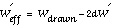
Wdrawn = W * WMULT + XW
Ldrawn = L * LMULT + XL
where the unprimed
W
eff
is bias-dependent, and the primed quantity is bias-independent.
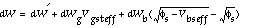
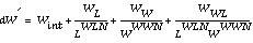
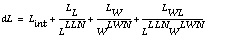
For C-V calculations dW' is replaced with
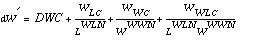
and dL' is replaced with
NOTE: A detailed discussion of the BSIM3 Version 3 equations is available from the BSIM3 site: http://www-device.eecs.berkeley.edu/~bsim3/get.html
.MODEL CARDS NMOS Model
.model nch nmos LEVEL=49
+ Tnom=27.0
+ nch=1.024685E+17 tox=1.00000E-08 xj=1.00000E-07
+ lint=3.75860E-08 wint=-2.02101528644562E-07
+ vth0=.6094574 k1=.5341038 k2=1.703463E-03 k3=-17.24589
+ dvt0=.1767506 dvt1=.5109418 dvt2=-0.05
+ nlx=9.979638E-08 w0=1e-6
+ k3b=4.139039
+ vsat=97662.05 ua=-1.748481E-09 ub=3.178541E-18 uc=1.3623e-10
+ rdsw=298.873 u0=307.2991 prwb=-2.24e-4
+ a0=.4976366
+ keta=-2.195445E-02 a1=.0332883 a2=.9
+ voff=-9.623903E-02 nFactor=.8408191 cit=3.994609E-04
+ cdsc=1.130797E-04
+ cdscb=2.4e-5
+ eta0=.0145072 etab=-3.870303E-03
+ dsub=.4116711
+ pclm=1.813153 pdiblc1=2.003703E-02 pdiblc2=.00129051
+ pdiblcb=-1.034e-3
+ drout=.4380235 pscbe1=5.752058E+08 pscbe2=7.510319E-05
+ pvag=.6370527 prt=68.7 ngate=1.e20 alpha0=1.e-7 beta0=28.4
+ prwg=-0.001 ags=1.2
+ dvt0w=0.58 dvt1w=5.3e6 dvt2w=-0.0032
+ kt1=-.3 kt2=-.03
+ at=33000
+ ute=-1.5
+ ua1=4.31E-09 ub1=7.61E-18 uc1=-2.378e-10
+ kt1l=1e-8
+ wr=1 b0=1e-7 b1=1e-7 dwg=5e-8 dwb=2e-8 delta=0.015
+ cgdl=1e-10 cgsl=1e-10 cgbo=1e-10 xpart=0.0
+ cgdo=0.4e-9 cgso=0.4e-9
+ clc=0.1e-6
+ cle=0.6
+ ckappa=0.6
PMOS Model
This is an example of a PMOS model. Note that VTH0 is negative.
.model pch PMOS LEVEL=49
+ Tnom=27.0
+ nch=5.73068E+16 tox=1.00000E-08 xj=1.00000E-07
+ lint=8.195860E-08 wint=-1.821562E-07
+ vth0=-.86094574 k1=.341038 k2=2.703463E-02 k3=12.24589
+ dvt0=.767506 dvt1=.65109418 dvt2=-0.145
+ nlx=1.979638E-07 w0=1.1e-6
+ k3b=-2.4139039
+ vsat=60362.05 ua=1.348481E-09 ub=3.178541E-19 uc=1.1623e-10
+ rdsw=498.873 u0=137.2991 prwb=-1.2e-5
+ a0=.3276366
+ keta=-1.8195445E-02 a1=.0232883 a2=.9
+ voff=-6.623903E-02 nFactor=1.0408191 cit=4.994609E-04
+ cdsc=1.030797E-3
+ cdscb=2.84e-4
+ eta0=.0245072 etab=-1.570303E-03
+ dsub=.24116711
+ pclm=2.6813153 pdiblc1=4.003703E-02 pdiblc2=.00329051
+ pdiblcb=-2.e-4
+ drout=.1380235 pscbe1=0 pscbe2=1.e-28
+ pvag=-.16370527
+ prwg=-0.001 ags=1.2
+ dvt0w=0.58 dvt1w=5.3e6 dvt2w=-0.0032
+ kt1=-.3 kt2=-.03 prt=76.4
+ at=33000
+ ute=-1.5
+ ua1=4.31E-09 ub1=7.61E-18 uc1=-2.378e-10
+ kt1l=0
+ wr=1 b0=1e-7 b1=1e-7 dwg=5e-8 dwb=2e-8 delta=0.015
+ cgdl=1e-10 cgsl=1e-10 cgbo=1e-10 xpart=0.0
+ cgdo=0.4e-9 cgso=0.4e-9
+ clc=0.1e-6
+ cle=0.6
+ ckappa=0.6
Star-Hspice Manual - Release 2001.2 - June 2001