LEVEL 47 BSIM3 Version 2 MOS Model
The BSIM3 version 2.0 MOS model from UC Berkeley is available as the LEVEL 47 Star-Hspice model.
LEVEL 47 Model Parameters
|
Name
|
Unit
|
Default
|
Description
|
|
VTH0
|
V
|
0.7
|
Threshold voltage of long channel at
Vbs
= 0
and small
Vds
(0.7 for n-channel, - 0.7 for p-channel)
|
|
K1
|
V
1/2
|
0.53
|
First-order body effect coefficient
|
|
K2
|
|
-0.0186
|
Second-order body effect coefficient
|
|
K3
|
|
80.0
|
Narrow width effect coefficient
|
|
K3B
|
1/V
|
0
|
Body width coefficient of narrow width effect
|
|
KT1
|
V
|
-0.11
|
Temperature coefficient for threshold voltage
|
|
KT2
|
|
0.022
|
Body bias coefficient of threshold temperature effect
|
|
GAMMA1
|
V
1/2
|
See "LEVEL 47 Model Equations"
|
Body effect coefficient, near interface
|
|
GAMMA2
|
V
1/2
|
See "LEVEL 47 Model Equations"
|
Body effect coefficient in the bulk
|
|
W0
|
m
|
2.5e-6
|
Narrow width effect coefficient
|
|
NLX
|
m
|
1.74e-7
|
Lateral nonuniform doping along channel
|
|
TOX
|
m
|
150e-10
|
Gate oxide thickness
|
|
XJ
|
m
|
0.15e-6
|
Junction depth
|
|
DL
|
m
|
0.0
|
Channel length reduction on one side (multiplied by SCALM)
|
|
DW
|
m
|
0.0
|
Channel width reduction on one side (multiplied by SCALM)
|
|
NPEAK
|
cm
-3
(see The model parameters NPEAK and U0 can be entered in meters or centimeters. NPEAK is converted to cm-3 as follows: if NPEAK is greater than 1e20, it is multiplied by 1e-6. U0 is converted to m2/Vsec as follows: if U0 is greater than 1, it is multiplied by 1e-4. You must enter the parameter NSUB in cm-3 units.)
|
1.7e17
|
Peak doping concentration near interface
|
|
NSUB
|
cm
-3
|
6.0e16
|
Substrate doping concentration
|
|
PHI
|
V
|
See "LEVEL 47 Model Equations"
|
Surface potential under strong inversion
|
|
XT
|
m
|
1.55e-7
|
Doping depth
|
|
VBM
|
V
|
-5.0
|
Maximum substrate bias
|
|
VBX
|
V
|
See "LEVEL 47 Model Equations"
|
Vbs at which the depletion width equals XT
|
|
DVT0
|
|
2.2
|
Short-channel effect coefficient 0
|
|
DVT1
|
|
0.53
|
Short-channel effect coefficient 1
|
|
DVT2
|
1/V
|
-0.032
|
Short-channel effect coefficient 2
|
|
U0
|
m
2
/Vsec (see The model parameters NPEAK and U0 can be entered in meters or centimeters. NPEAK is converted to cm-3 as follows: if NPEAK is greater than 1e20, it is multiplied by 1e-6. U0 is converted to m2/Vsec as follows: if U0 is greater than 1, it is multiplied by 1e-4. You must enter the parameter NSUB in cm-3 units.)
|
0.067
|
Low field mobility at T = TREF
(0.067 for n-channel, 0.025 for p-channel)
|
|
UA
|
m/V
|
2.25e-9
|
First-order mobility degradation coefficient
|
|
UA1
|
m/V
|
4.31e-9
|
Temperature coefficient of UA
|
|
UB
|
m
2
/V
2
|
5.87e-19
|
Second-order mobility degradation coefficient
|
|
UB1
|
m
2
/V
2
|
-7.61e-18
|
Temperature coefficient of UB
|
|
UC
|
1/V
|
0.0465
|
Body bias sensitivity coefficient of mobility
|
|
UC1
|
1/V
|
-0.056
|
Temperature coefficient of UC
|
|
VSAT
|
cm/sec
|
8e6
|
Saturation velocity of carrier at T = TREF
|
|
AT
|
m/sec
|
3.3e4
|
Temperature coefficient of VSAT
|
|
RDSW
|
ohm
·
µm
|
0.0
|
Source drain resistance per unit width
|
|
RDS0
|
ohm
|
0.0
|
Source drain contact resistance
|
|
LDD
|
m
|
0.0
|
Total length of LDD region
|
|
ETA
|
|
0.3
|
Coefficient of drain voltage reduction
|
|
ETA0
|
|
0.08
|
Subthreshold region DIBL (Drain Induced Barrier Lowering) coefficient
|
|
ETAB
|
1/V
|
-0.07
|
Subthreshold region DIBL coefficient
|
|
EM
|
V/m
|
4.1e7
|
Electrical field in channel above which hot carrier effect dominates
|
|
NFACTOR
|
|
1.0
|
Subthreshold region swing
|
|
VOFF
|
V
|
-0.11
|
Offset voltage in subthreshold region
|
|
LITL
|
m
|
|
Characteristic length. The default is
|
|
VGLOW
|
V
|
-0.12
|
Lower bound of the weak-strong inversion transition region
|
|
VGHIGH
|
V
|
0.12
|
Upper bound of the weak-strong inversion transition region
|
|
CDSC
|
F/m
2
|
2.4e-4
|
Drain/source and channel coupling capacitance
|
|
CDSCB
|
F/Vm
2
|
0
|
Body coefficient for CDSC
|
|
CIT
|
F/m
2
|
0.0
|
Interface state capacitance
|
|
PCLM
|
|
1.3
|
Coefficient of channel length modulation
|
|
PDIBL1
|
|
0.39
|
DIBL (Drain Induced Barrier Lowering) effect coefficient 1
|
|
PDIBL2
|
|
0.0086
|
DIBL effect coefficient 2
|
|
DROUT
|
|
0.56
|
DIBL effect coefficient 3
|
|
DSUB
|
|
DROUT
|
DIBL coefficient in subthreshold region
|
|
PSCBE1
|
V/m
|
4.24e8
|
Substrate current induced body effect exponent 1
|
|
PSCBE2
|
m/V
|
1.0e-5
|
Substrate current induced body effect coefficient 2
|
|
A0
|
|
1
|
Bulk charge effect. The default is 4.4 for PMOS.
|
|
TNOM (TREF)
|
°C
|
25
|
Temperature at which parameters are extracted. This parameter defaults to the option TNOM, which defaults to 25 °C. See 4 and 5 in "Reminders for this Installation," below.
|
|
SUBTHMOD
|
|
2
|
Subthreshold model selector
|
|
SATMOD
|
|
2
|
Saturation model selector
|
|
KETA
|
1/V
|
-0.047
|
Body bias coefficient of the bulk charge effect
|
|
A1
|
1/V
|
0
|
First nonsaturation factor (0 for NMOS, 0.23 for PMOS)
|
|
A2
|
|
1.0
|
Second nonsaturation factor (1.0 for NMOS, 0.08 for PMOS)
|
|
UTE
|
|
-1.5
|
Mobility temperature exponent
|
|
KT1L
|
Vm
|
0
|
Channel length sensitivity of temperature coefficient for threshold voltage
|
|
UC0*
|
(V/m)
2
|
|
Temperature coefficient
|
|
BULKMOD
|
|
1
|
Bulk charge model selector
|
|
XPART
|
|
1
|
Charge partitioning flag
|
|
VFB
|
V
|
|
Flat-band voltage
|
|
PVAG
|
|
0
|
Gate dependence of output resistance
|
|
* UC0 has no effect on the model
|
Using the BSIM3 Version 2 MOS Model in Star-Hspice
The Star-Hspice LEVEL 47 model uses the same model parameters for source/drain diode current, capacitance, and resistance as do the other Star-Hspice MOS levels. The model parameter ACM controls the choice of source/drain equations.
The Star-Hspice LEVEL 47 model also uses the same noise equations as the other levels. The parameter NLEV controls the choice of noise equations.
This model, like all models in Star-Hspice, can be parametrized. This is useful for modeling process skew, either by worst-case corners or by Monte Carlo. For information on worst-case and Monte Carlo analysis, see Performing Worst Case Analysis and Performing Monte Carlo Analysis.
Notes:
1. Set LEVEL=47 to identify the model as a BSIM3 model.
2. This model is based on BSIM3 version 2.0 from UC Berkeley. Code was received from UC Berkeley in July 1994, in the form of SPICE3e2. Changes announced in a letter from UCB September 13, 1994, have been included. DC sweeps have been checked against SPICE3e2.
3. The default setting for CAPOP is CAPOP=13, which is the BSIM1 charge-conserving capacitance model. The BSIM3 capacitance model has not been installed.
4. The LEVEL 47 model supports the model parameter name TNOM as an alias for TREF. The conventional terminology in Star-Hspice is TREF, which is supported as a model parameter in all Star-Hspice MOS levels. The alternative name TNOM is supported for LEVEL 47, for compatibility with SPICE3.
5. The default room temperature is 25°C in Star-Hspice, but is 27°C in SPICE3. If the BSIM3 model parameters are specified at 27°C, TREF=27 should be added to the model, so that the model parameters is interpreted correctly. It is a matter of choice whether or not to set the nominal simulation temperature to 27, by adding .OPTION TNOM=27 to the netlist. This should be done when testing Star-Hspice versus SPICE3.
6. The default of DERIV is zero, the analytical method. DERIV can be set to 1 for the finite difference method. The analytic derivatives in the SPICE3e2 code are not exact in some regions. Setting DERIV=1 gives more accurate derivatives (GM, GDS, GMBS), but consumes more CPU time.
7. There are three ways for the BSIM3 model to calculate Vth:
-
Using K1 and K2 values that are user specified
-
Using GAMMA1, GAMMA2, VBM, and VBX values entered in the .MODEL statement
-
Using NPEAK, NSUB, XT, and VBM values that are user specified
8. The model parameters NPEAK and U0 can be entered in meters or centimeters. NPEAK is converted to cm-3 as follows: if NPEAK is greater than 1e20, it is multiplied by 1e-6. U0 is converted to m2/Vsec as follows: if U0 is greater than 1, it is multiplied by 1e-4. You must enter the parameter NSUB in cm-3 units.
9. The specified value of VTH0 for p-channel in the .MODEL statement should be negative.
10. The default value of KT1 is -0.11. The negative sign ensures that the absolute value of threshold decreases with increasing temperature for NMOS and PMOS.
11. Model parameter LITL is not allowed to go below a minimum value of 1.0e-9 m, to avoid a possible divide by zero error.
12. VSAT, after temperature adjustment, is not allowed to go below a minimum value of 1.0e4 m/sec, to assure that it is positive after temperature compensation.
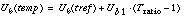
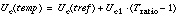
13. There are seven model parameters for accommodating the temperature dependencies of six temperature dependent model variables. They are KT1 and KT2 for VTH, UTE for U0, AT for VSAT, UA1 for UA, UB1 for UB, and UC1 for UC.
14. Set up the conversion of temperature between Star-Hspice and SPICE3 as follows:
SPICE3: .OPTIONS TEMP=125
.MODEL NCH NMOS LEVEL=8
+ TNOM =27 ...
HSPICE: .TEMP 125
.MODEL NCH NMOS LEVEL=47
+ TREF =27 ...
15. The option SCALM does not affect the parameters unique to this model, but it does affect the common MOS parameters, such as XL, LD, XW, WD, CJ, CJSW, JS, and JSW.
16. LEVEL 47 uses the common Star-Hspice MOS parasitic models, specified by ACM.
17. LEVEL 47 uses the common Star-Hspice MOS noise models, specified by NLEV.
18. DELVTO and DTEMP on the element line can be used with LEVEL 47.
19. The impact ionization current determined by the model parameters PSCBE1 and PSCBE2 contributes to the drain-source current; it does not contribute to bulk current.
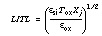
Leff and Weff Equations for BSIM3 Version 2.0
The standard Star-Hspice equations for Leff and Weff are:
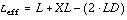
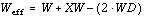
The UCB SPICE3 equations used for BSIM3 are:
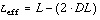
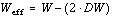
The units for these parameters are meters, with defaults of zero.
Star-Hspice uses the standard Star-Hspice equation for both cases, and accepting DL(DW) as the value for LD(WD). If both LD(WD) and DL(DW) are specified in an Star-Hspice .MODEL statement, Star-Hspice uses the LD(WD) value.
If LDAC and WDAC are included in the .MODEL statement,
Leff = L+XL-2·LDAC, Weff = W+XW-2·WDAC
The model uses the values of LD(DL) and WD(DW) to generate defaults for CGSO, CGDO, and CGBO. The values are also used with parameters RS and RD for ACM>0.
Example
The following two models give the same Star-Hspice results:
* HSPICE style:
.MODEL n1 nmos LEVEL=47 XL=0.1e6 LD=0.15e-6
+ SatMod=2 SubthMod=2 BulkMod=1
+ CGSO=0.3e-9 CGDO=0.3e-9 CGBO=0
* SPICE3 style:
.MODEL n2 nmos LEVEL=47 LD=0.1e-6
+ SatMod=2 SubthMod=2 BulkMod=1
+ CGSO=0.3e-9 CGDO=0.3e-9 CGBO=0
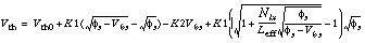
LEVEL 47 Model Equations
The following model equations are based on the source code of BSIM3.
Threshold Voltage
Model Parameters

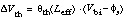
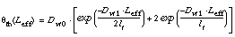
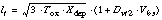
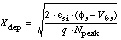
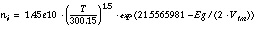
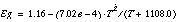
If Phis is not specified as a model parameter, then
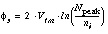 (Npeak and ni in cm-3)

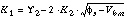
If K1, K2 are not specified as model parameters, then they are calculated as follows:
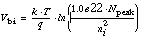
If Vbi is not specified as a model parameter, then
Mobility of Carrier
Model Parameters

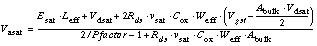
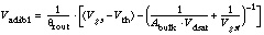
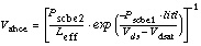
Drain Saturation Voltage
Model Parameters
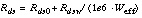
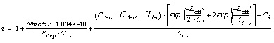
Rds and Pfactor:
 (if Pfactor > 1, it is set to Pfactor = 1)

Vdsat for the case Rds = 0 and Pfactor = 1:
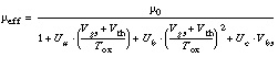
For BULKMOD = 1,
For BULKMOD = 2,

For Vbs
<=
0,

For Vbs >= 0,


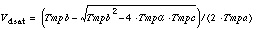
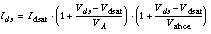
Vdsat for the general case:
Vdsat is the solution of Tmpa * Vdsat * Vdsat - Tmpb * Vdsat + Tmpc = 0


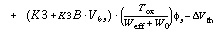
Linear Region

Saturation Region
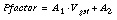
Model Parameters

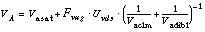
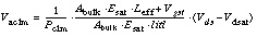
Vasat and Fvag:
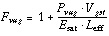
Early Voltage, satMod = 1:
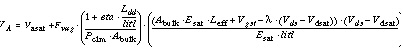
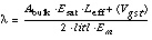
Early Voltage, satMod = 2:

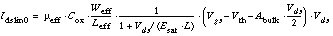
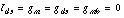
Drain Current

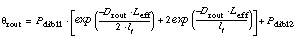
Subthreshold Region
Model Parameters

n and DIBL:
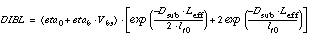


If subthMod = 0,
If subthMod = 1,
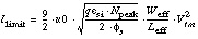
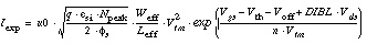
If subthMod = 2,

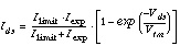
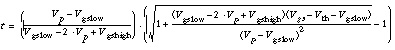
Transition Region (for subthMod = 2 only)
Model Parameters


Temperature Compensation
Model Parameters


PMOS Model
The following is an example of a PMOS model. Note that VTH0 is negative.
.model pch PMOS LEVEL=47
+ Tnom=27.0
+ Npeak= 1.5E+23 Tox=7.0E-09 Xj=1.0E-07
+ dl= 0.2E-06 dw=-0.1E-06
+ SatMod= 2 SubthMod= 2 BulkMod= 1
+ Vth0= -.8 Phi= .7 K1= .5 K2=0.03 K3= 0
+ Dvt0= 48 Dvt1= .6 Dvt2=-5e-4
+ Nlx=0 W0= 0
+ Vsat= 9E6 Ua= 1E-09 Ub= 0 Uc= -3E-02
+ Rds0= 180 Rdsw= 0 U0= 7E-03
+ A0= .87
+ Voff=-.07 NFactor= 1.5 Cit=-3E-05
+ Cdsc= 6E-02 Vglow=-.12 Vghigh= .12
+ Pclm= 77 Pdibl1= 0 Pdibl2= 2E-011
+ Drout= 0 Pscbe1= 0 Pscbe2= 1E-28
+ Eta= 0 Litl= 4.5E-08
+ Em= 0 Ldd= 0
+ kt1=-.3 kt2=-.03
+ At= 33000
+ Ua1= 4E-09 Ub1= 7E-18 Uc1= 0
Star-Hspice Manual - Release 2001.2 - June 2001