


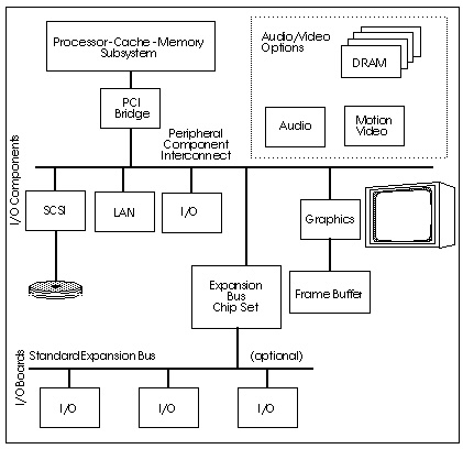
Peripheral Component Interconnect (PCI) is an interconnect specification for standard personal computer architectures. PCI enables low-cost, high-performance standard I/O functions (PCI System Block Diagram). PCI provides a component-level standard, contrasted to EISA/ISA board-level standards. Both standards coexist with higher performance functions integrated into the system on PCI, while EISA/ISA bring end users the flexibility of adding lower bandwidth functions.
PCI's targeted frequency allows it to achieve higher performance. At its target speed, a significant part of the cycle time is spent in the actual propagation of the signals through the system. Use an analog simulation of the interconnect to understand this phenomenon. Star-Hspice is ideally suited to resolving PCI design issues because of the following capabilities:
All of these advanced features are used extensively throughout the models and processes described here.
Intel's PCI Speedway is a recommended method for interconnecting PCI devices, as shown in PCI Speedway. The Speedway is not the only way to interconnect PCI devices, but it has proven to be a robust solution.
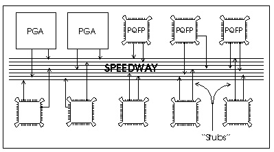
PCI Speedway shows ten PCI devices connected together through a narrow band of traces referred to as the "Speedway." Each device's PCI signals connect to the Speedway through a short trace on an orthogonal layer known as a "stub". If the stubs are short enough, they do not cause any unwanted interruptions to a signal traveling on the Speedway except to slow it down.
The PCI Speedway implementation places components on both sides of the Speedway, spaced every two inches, causing a signal traveling on the Speedway to see a new load every inch (on average). This stub-to-stub element is referred to as a "line". Consequently, the Speedway trace is actually a collection of "lines". Both lines and stubs are fully expressed in the Star-Hspice model named and described below.
The Speedway is a behavioral representation of integrated outputs and inputs to speed the simulations and achieve a greater amount of investigation. These elements simulate 25 times faster than silicon models and allow the invention of an optimal PCI buffer characteristic and specification. These buffers are currently provided for use in encrypted form.
The PCI files provided under Star-Hspice are listed in PCI-HSPICE Files. These are the same files that were derived at Intel Corporation. You can find these files under the \meta\<release>\parts\pci directory in the PC version of Star-Hspice, or the $installdir/parts/pci directory in other version of Star-Hspice. They are available on all common computers and operating systems.
The .inc files are all called by the .sp files during simulation. Consequently, they need to be in the current directory or in a directory referenced by the hspice.ini file search statements.
The worst-case PCI Speedway reference file, pci_wc.sp , can be used directly, or customized to match other PCI implementations. The file serves as a template for experimentation to investigate other configurations. The file also serves as a quick guide to learning the advanced features of Star-Hspice, and seeing them in action.
The reference PCI Speedway file is well documented, to make it simple to use and customize. Hardcopy of this file is listed in PCI Simulation Example Files. The file is broken into six major sections, as listed below:
This is the same order that sections appear in the file. The following sections provide a short explanation of each file section, along with actual examples from the file.
The PCI model makes extensive use of "parameter" (.PARAM) statements to allow you to describe the environment in a few specific places rather than throughout the file. An example of a parameter is the system voltage. Once the parameter is defined in the Parameter section of the file, you can use it in numerous places throughout the file without further editing. This greatly simplifies the creation of new files, with little or no understanding of the actual circuit section.
Three subsections define the system, line, and stub parameters. The system parameters are listed here:
.param vccdc=5.00V $ system voltage
.param per=60ns $ period of pulse generator
.param v0=0V vp=5V $ amplitude of pulse generator
.param trp=2.5ns $ rise time of pulse generator
.param tfp='trp' $ fall time of pulse generator
.param tw='(per/2)-trp' $ pulse width of pulse generator
.param td=2ns $ delay time of pulse generator
.param cvia=0.5pF $ via capacitance where stub hits speedway
.param Cin=8.0pF $ input capacitance of buffer
.param Ci_pkg=2.0pF $ package capacitance on input of buffer
.param Li_pkg=8nH $ input bond wire inductance of buffer
.param Ri_pkg=0.03 $ input pin/bond-wire resistance
As the comments show, you can set various system parameters such as the DC voltage and the frequency/waveshape of the applied pulse generator. This waveform is applied to the input of the output buffer under test. You can also set the amount of a capacitance applied to a via (the connection of a trace from one layer to the next) using the appropriate parameter.
The last four parameters are passed to the input load model and allow you to see the effects of various packages and loads on Speedway performance. The reference file has ten input loads on the Speedway at the end of the "stub" traces.
The next set of parameters describe the printed circuit board fabrication of the "line" elements. As previously described, the "line" traces make up the Speedway length and connect the "stubs" together. Star-Hspice uses these dimensions to develop a lossy transmission line model of the printed circuit traces. This model accurately characterizes the intrinsic impedance and propagation velocity of the trace, as fabricated.
.param line=1.0 $ line length, in inches
.param linewd=6 $ line width, in mils
.param lineht=16 $ line height from ground plane, in mils
.param lineth=2.0 $ line thickness, in mils
.param linelyr=0 $ line layer, 1=outer 0=inner
The values shown here represent a 6 mil trace on an inner layer, 16 mils from the ground plane. Assuming the components are spaced every two inches on both sides of the speedway, the line length would be one inch as shown. If the components were more spread out, you could set the length using the parameter "line". The stub parameters are similar to the line parameters, and are listed as follows:
.param stub=1.5 $ length of stub, in inches
.param stubwd=6 $ stub width, in mils
.param stubht=20 $ stub height from ground plane, in mils
.param stubth=1.8 $ stub thickness, in mils
.param stublyr=1 $ stub layer, 1=outer 0=inner
Here, the stubs are set on an outer layer, with a length of 1.5 inches (the recommended maximum).
The following statements cause Star-Hspice to perform a transient analysis, ending the simulation at 60 ns:
The .PROBE statements store the transient voltage observed during simulation at the load specified and are similar to placing an oscilloscope probe at that point on a physical board. The waveforms at all ten loads are saved, in addition to the 50 pF reference.
During simulation, Star-Hspice automatically measures T_prop (as defined by the PCI specification), using the .MEASURE statement. The reference file contains .MEASURE commands for rising edge and falling edge measurements. The simulation measures and saves the time delay in a file with a .mt0 extension. Note that if you run a falling edge simulation, the rising edge measurements are invalid. Similarly, if you run a rising edge simulation, the falling edge measurements are invalid. This is important to remember when referring to the .mt0 file after a simulation.
Examples of the .MEASURE statements from the file are listed here.
*************************************************************
* Rising edge T_prop measurements *
*****************************************************************
.MEAS tran tr1_val TRIG V(ref_50pf) val=1.5v td='per/2' cross=1
+ TARG V(load1) val=2.0v rise=last
.MEAS tran tr2_val TRIG V(ref_50pf) val=1.5v td='per/2' cross=1
+ TARG V(load2) val=2.0v rise=last...
.MEAS tran tr10_val TRIG V(ref_50pf) val=1.5v td='per/2' cross=1
+ TARG V(load10) val=2.0v rise=last
***************************************************************** Falling edge T_prop measurements * **************************************************************
.MEAS tran tf1_val TRIG V(ref_50pf) val=1.5v td='per/2' cross=1
+ TARG V(load1) val=0.8v fall=last...
.MEAS tran tf10_val TRIG V(ref_50pf) val=1.5v td='per/2' cross=1
+ TARG V(load10) val=0.8v fall=last
The file provides .MEASURE statements to measure T_prop from the ref_50pf waveform to each of ten loads. Since each load is measured, you can quickly determine the worst-case T_prop for a given configuration by finding the largest value.
The .MEASURE statements work by triggering on the ref_50pf signal as it crosses 1.5 volts and ending the measurement when the target waveform crosses the specified voltage for the last time. For rising edge measurements, this value is 2.0 volts. For falling edge measurements, the value is 0.8 volts.
Use the Speedway file to quickly test numerous buffers by acquiring or creating a subcircuit file of the desired buffer and inserting the name into the file. Then you can drive the Speedway from any load position.
The following file shows that the driver chosen is a worst-case Class II buffer. Note that the file uses two buffers; one drives the Speedway from load1, and the other drives a simple 50 pf reference load.
*********************************************************************
* PCI Driver Selection *
* *
* To drive the Speedway from another load position, change the *
* next line. For example the statement: *
* *
* Vdrvout load2 drvout $ driver position and current *
* *
* would drive the Speedway from position number two. The driver *
* model should be formed into a subcircuit, called from the lines *
* *
* Xdriver sqwave drvout VCC GND xxxx $ place driver here *
* Xref_drv sqwave ref_50pf VCC GND xxxx $ place driver here too*
* *
* where "xxxx" represents the driver subcircuit name. The nodes *
* must be placed in the order: input output vcc gnd. *
* *
* *
* change *
* position *
* here *
*********************************************************************
Vdrvout  load1
  drvout						$ driver pos'n and current
Xdriver sqwave drvout VCC GND PCI_II_W $ place driver here
Xref_drv sqwave ref_50pf VCC GND PCI_II_W $ place driver here too
* in out vcc gnd name $ driver format
Xref_clamp ref_50pf VCC 0 PCI_IN_W $ need input structure
Cref_cap ref_50pf 0 '50e-12-(Cin+Ci_pkg)' $ total cap. = 50pf
Vpulse sqwave 0 PULSE v0 vp td trp tfp tw per
Vsupply VCC 0 DC VCCDC
To understand the reference driver and the Speedway subsections, refer to PCI Speedway Circuit Schematic.
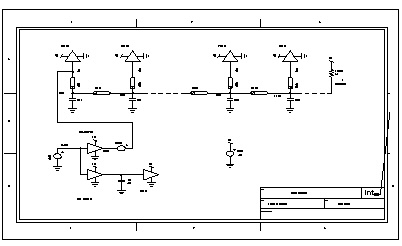
This figure shows the overall topology of the Speedway, and how the individual elements are interconnected.
Aside from the driver section, the Speedway is made up of repetitive subsections, represented in the file as listed below (for the Load 2 and 3 subsections):
*********************************************************************
* Speedway Sub-section Load 2 *
*********************************************************************
Xline1_2 stub1 stub2 TRACE LENGTH=line
+ W=LINEWD H=LINEHT T=LINETH DLEVOUT=LINELYR CORRECT=1
Xstub2 stub2 load2 TRACE LENGTH=STUB
+ W=STUBWD H=STUBHT T=STUBTH DLEVOUT=STUBLYR CORRECT=1
Xload2 load2 VCC 0 PCI_IN_W
Cvia2 stub2 0 CVIA
*********************************************************************
* Speedway Sub-section Load 3 *
*********************************************************************
Xline2_3 stub2 stub3 TRACE LENGTH=LINE
+ W=LINEWD H=LINEHT T=LINETH DLEVOUT=LINELYR CORRECT=1
Xstub3 stub3 load3 TRACE LENGTH=STUB
+ W=STUBWD H=STUBHT T=STUBTH DLEVOUT=STUBLYR CORRECT=1
Xload3 load3 VCC 0 PCI_IN_W
Cvia3 stub3 0 CVIA
As shown in the figure and the listing, each subsection consists of a "line" from the previous subsection (for example, Xline2_3 joins subsections two and three together), a "stub" to the load, a load model at the end of the stub, and a trace via where the stub meets the line. Each element is defined by parameters at the top of the file, but you could adjust it by replacing the parameter name with a value instead. This flexibility is particularly useful since the stubs and lines do not normally have the same length.
You can simulate PCI implementations with fewer than ten loads by either deleting subsections or commenting them out with an asterisk (*) at the beginning of the line
When the .ALTER statement is invoked, Star-Hspice automatically alters a file and resimulates. The reference file uses this feature at the end to force a rising edge simulation. For the worst-case rising edge simulation, reset the system voltage to its minimum tolerance. In addition, invert the applied input pulse as shown in the following code excerpt.
*********************************************************************
* Alter for Class_II (rising edge) *
*********************************************************************
.alter
.param vccdc=4.75V $ set system voltage here
.param v0=5V vp=0V $ amplitude of pulse generator
Additional .ALTER statements can change the driver type, as shown here to test the falling edge of a best-case PCI driver.
*********************************************************************
* Alter for Best-Case Class_II Driver (falling edge) *
*********************************************************************
.alter
.param vccdc=5.25V $ set system voltage here
.param v0=0V vp=5V $ amplitude of pulse gen.
Xdriver sqwave drvout VCC GND PCI_II_B $ place driver here
Xref_drv sqwave ref_50pf VCC GND PCI_II_B $ place driver here too
*********************************************************************
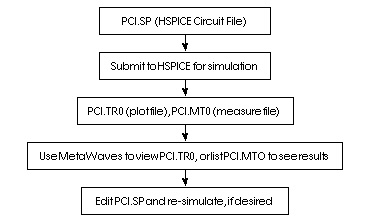
The following outline and examples of simulations help you to understand PCI Star-Hspice simulation. These acquaint you with the simulation process and demonstrate how to adapt the file to simulate other topologies or variations.
The simulation process is outlined as follows:
The following list provides ideas for simulation options. Use any combination of the changes listed here, or try your own. Values to change are underlined.
1. To drive the Speedway from another location (other than position #1), change:
Vdrvout load1 drvout $ driver pos'n and current
Vdrvout  load4
  drvout						$ driver pos'n and current
To convert the topology from a "Speedway" to a "Subway" (traces run under the components), change:
.param stub=1.5
						$ length of stub, in inches
.param line=1.0
						$ line length, in inches
.param stub=0.25
					$ length of stub, in inches
.param line=2.0
						$ line length, in inches
To change the primary printed circuit fabrication parameters on the Speedway traces, change:
.param linewd=6
						$ line width, in mils
.param lineht=16
						$ line height from ground plane, in mils
.param linewd=10
						$ line width, in mils
.param lineht=8
						$ line height from ground plane, in mils
To make one of the stubs abnormally long (example would make the stub to device #7 8"), change:
Xstub7 stub7 load7 TRACE LENGTH=STUB
Xstub7 stub7 load7 TRACE LENGTH=8
Hardcopy of PCI_WC.SP Simulation File
PCI Speedway, 10-load Reference Model, Worst-Case (file=PCI_WC.SP)
**********************************************************************
**********************************************************************
** COPYRIGHT 1992 Intel Corporation **
** Version: 1.7 **
**********************************************************************
**********************************************************************
* *
* This is a base model of the PCI Speedway environment developed *
* under HSPICE. Most pertinent environment attributes have been *
* reduced to HSPICE "parameters." For example, system voltage can *
* be set simply by typing the desired voltage on the line: *
* *
* .param vccdc=??.?V $ set system voltage here *
* *
* The file is structured with the following sections (in order): *
* *
* 1. Parameters *
* 2. HSPICE Control/Analysis Statements *
* 3. Measure Commands *
* 4. PCI Driver Selection *
* 5. PCI Speedway Subsections *
* 6. File Alter Commands *
* *
**********************************************************************
* Interconnect Topology Explanation *
* *
* The PCI Speedway interconnects 10 integrated circuit components *
* through a network of "stubs" and "lines" as shown: *
* *
* 1 2 3 4 5 6 7 8 9 10 *
* |____|____|____|____|____|____|____|____|____| *
* *
* where, *
* stub = | *
* line = ____ *
* *
* Each IC load "stubs" onto the Speedway, which is really just a *
* collection of "lines". "Line" length represents the physical *
* part-to-part spacing. "Stub" length is the distance from the *
* component lead to appropriate trace on the speedway. On a *
* printed circuit board, "lines" will typically be routed on *
* horizontal layers, and "stub" on vertical layers. As such, the *
* geometric parameters for both "stubs" and "lines" (width, *
* distance to the ground plane, ...) are adjustable below. *
**********************************************************************
* File Control Parameters *
**********************************************************************
.param vccdc=4.75V $ set system voltage here
.param per=60ns $ period of pulse generator
.param v0=5V vp=0V $ amplitude of pulse generator
.param trp=2.5ns $ rise time of pulse generator
.param tfp='trp' $ fall time of pulse generator
.param tw='(per/2)-trp' $ pulse width of pulse generator
.param tdly=2ns $ delay time of pulse generator
.param cvia=0.5pF $ via capacitance where stub hits speedway
.param Cin=8.0pF $ input capacitance of buffer
.param Ci_pkg=2.0pF $ package capacitance on input of buffer
.param Li_pkg=8nH $ input bond wire inductance of buffer
.param Ri_pkg=0.03 $ input pin/bond-wire resistance
**********************************************************************
* Cin + Ci_pkg should equal 10 pF max (PCI Spec C_i/o).
**********************************************************************
* Line Trace Parameters *
**********************************************************************
.param line=1.0 $ line length, in inches
.param linewd=6 $ line width, in mils
.param lineht=16 $ line height from ground plane, in mils
.param lineth=2.0 $ line thickness, in mils
.param linelyr=0 $ line layer, 1=outer 0=inner
**********************************************************************
* Stub Trace Parameters *
**********************************************************************
.param stub=1.5 $ length of stub, in inches
.param stubwd=6 $ stub width, in mils
.param stubht=20 $ stub height from ground plane, in mils
.param stubth=1.8 $ stub thickness, in mils
.param stublyr=1 $ stub layer, 1=outer 0=inner
**********************************************************************
* Output Control Statements *
**********************************************************************
.TRAN 0.1ns 60ns
.OPTIONS ACCT RELTOL=.001 POST=1 PROBE
.PROBE ref_50pf=V(ref_50pf)
.PROBE load1=V(load1)
.PROBE load2=V(load2)
.PROBE load3=V(load3)
.PROBE load4=V(load4)
.PROBE load5=V(load5)
.PROBE load6=V(load6)
.PROBE load7=V(load7)
.PROBE load8=V(load8)
.PROBE load9=V(load9)
.PROBE load10=V(load10)
**********************************************************************
* The following lines can be used to measure the output current of *
* the driver and the impedance seen by the driver. Note that the *
* impedance of rising and falling edges are calculated differently. *
* (Remove comment "*" if you want to use this feature.) *
*.PROBE drvcur=I(vdrvout) *
*.PROBE tdr_rise=par('abs(V(drvout)/I(vdrvout))') *
*.PROBE tdr_fall=par('abs((V(vcc)-V(drvout))/I(vdrvout))') *
**********************************************************************
* Rising edge T_prop measurements *
**********************************************************************
.MEAS tran tr1_val TRIG V(ref_50pf) val=1.5v td='per/2' cross=1
+ TARG V(load1) val=2.0v rise=last
.MEAS tran tr2_val TRIG V(ref_50pf) val=1.5v td='per/2' cross=1
+ TARG V(load2) val=2.0v rise=last
.MEAS tran tr3_val TRIG V(ref_50pf) val=1.5v td='per/2' cross=1
+ TARG V(load3) val=2.0v rise=last
.MEAS tran tr4_val TRIG V(ref_50pf) val=1.5v td='per/2' cross=1
+ TARG V(load4) val=2.0v rise=last
.MEAS tran tr5_val TRIG V(ref_50pf) val=1.5v td='per/2' cross=1
+ TARG V(load5) val=2.0v rise=last
.MEAS tran tr6_val TRIG V(ref_50pf) val=1.5v td='per/2' cross=1
+ TARG V(load6) val=2.0v rise=last
.MEAS tran tr7_val TRIG V(ref_50pf) val=1.5v td='per/2' cross=1
+ TARG V(load7) val=2.0v rise=last
.MEAS tran tr8_val TRIG V(ref_50pf) val=1.5v td='per/2' cross=1
+ TARG V(load8) val=2.0v rise=last
.MEAS tran tr9_val TRIG V(ref_50pf) val=1.5v td='per/2' cross=1
+ TARG V(load9) val=2.0v rise=last
.MEAS tran tr10_val TRIG V(ref_50pf) val=1.5v td='per/2' cross=1
+ TARG V(load10) val=2.0v rise=last
**********************************************************************
* Falling edge T_prop measurements *
**********************************************************************
.MEAS tran tf1_val TRIG V(ref_50pf) val=1.5v td='per/2' cross=1
+ TARG V(load1) val=0.8v fall=last
.MEAS tran tf2_val TRIG V(ref_50pf) val=1.5v td='per/2' cross=1
+ TARG V(load2) val=0.8v fall=last
.MEAS tran tf3_val TRIG V(ref_50pf) val=1.5v td='per/2' cross=1
+ TARG V(load3) val=0.8v fall=last
.MEAS tran tf4_val TRIG V(ref_50pf) val=1.5v td='per/2' cross=1
+ TARG V(load4) val=0.8v fall=last
.MEAS tran tf5_val TRIG V(ref_50pf) val=1.5v td='per/2' cross=1
+ TARG V(load5) val=0.8v fall=last
.MEAS tran tf6_val TRIG V(ref_50pf) val=1.5v td='per/2' cross=1
+ TARG V(load6) val=0.8v fall=last
.MEAS tran tf7_val TRIG V(ref_50pf) val=1.5v td='per/2' cross=1
+ TARG V(load7) val=0.8v fall=last
.MEAS tran tf8_val TRIG V(ref_50pf) val=1.5v td='per/2' cross=1
+ TARG V(load8) val=0.8v fall=last
.MEAS tran tf9_val TRIG V(ref_50pf) val=1.5v td='per/2' cross=1
+ TARG V(load9) val=0.8v fall=last
.MEAS tran tf10_val TRIG V(ref_50pf) val=1.5v td='per/2' cross=1
+ TARG V(load10) val=0.8v fall=last
**********************************************************************
* PCI Driver Selection *
* *
* To drive the Speedway from another load position, change the *
* next line. For example the statement: *
* *
* Vdrvout load2 drvout $ driver position and current *
* *
* would drive the Speedway from position number two. The driver *
* model should be formed into a subcircuit, called from the lines *
* *
* Xdriver sqwave drvout VCC GND xxxx $ place driver here *
* Xref_drv sqwave ref_50pf VCC GND xxxx $ place driver here too *
* *
* where "xxxx" represents the driver subcircuit name. The nodes *
* must be placed in the order: input ouput vcc gnd. *
* *
* *
* change *
* position *
* here *
**********************************************************************
Vdrvout load1 drvout $ driver pos'n and current
Xdriver sqwave drvout VCC GND PCI_II_W $ place driver here
Xref_drv sqwave ref_50pf VCC GND PCI_II_W $ place driver here too
* in out vcc gnd name $ driver format
Xref_clamp ref_50pf VCC 0 PCI_IN_W $ need input structure
Cref_cap ref_50pf 0 '50e-12-(Cin+Ci_pkg)' $ total cap. = 50pf
Vpulse sqwave 0 PULSE v0 vp tdly trp tfp tw per
Vsupply VCC 0 DC VCCDC
**********************************************************************
* Rpullup load10 VCC 1.5K $ use if appropriate
**********************************************************************
* Speedway Sub-section Load 1 *
**********************************************************************
Xstub1 stub1 load1 TRACE LENGTH=STUB
+ W=STUBWD H=STUBHT T=STUBTH DLEVOUT=STUBLYR CORRECT=1
Xload1 load1 VCC 0 PCI_IN_W
Cvia1 stub1 0 CVIA
**********************************************************************
* Speedway Sub-section Load 2 *
**********************************************************************
Xline1_2 stub1 stub2 TRACE LENGTH=line
+ W=LINEWD H=LINEHT T=LINETH DLEVOUT=LINELYR CORRECT=1
Xstub2 stub2 load2 TRACE LENGTH=STUB
+ W=STUBWD H=STUBHT T=STUBTH DLEVOUT=STUBLYR CORRECT=1
Xload2 load2 VCC 0 PCI_IN_W
Cvia2 stub2 0 CVIA
**********************************************************************
* Speedway Sub-section Load 3 *
**********************************************************************
Xline2_3 stub2 stub3 TRACE LENGTH=LINE
+ W=LINEWD H=LINEHT T=LINETH DLEVOUT=LINELYR CORRECT=1
Xstub3 stub3 load3 TRACE LENGTH=STUB
+ W=STUBWD H=STUBHT T=STUBTH DLEVOUT=STUBLYR CORRECT=1
Xload3 load3 VCC 0 PCI_IN_W
Cvia3 stub3 0 CVIA
**********************************************************************
* Speedway Sub-section Load 4 *
**********************************************************************
Xline3_4 stub3 stub4 TRACE LENGTH=LINE
+ W=LINEWD H=LINEHT T=LINETH DLEVOUT=LINELYR CORRECT=1
Xstub4 stub4 load4 TRACE LENGTH=STUB
+ W=STUBWD H=STUBHT T=STUBTH DLEVOUT=STUBLYR CORRECT=1
Xload4 load4 VCC 0 PCI_IN_W
Cvia4 stub4 0 CVIA
**********************************************************************
* Speedway Sub-section Load 5 *
**********************************************************************
Xline4_5 stub4 stub5 TRACE LENGTH=LINE
+ W=LINEWD H=LINEHT T=LINETH DLEVOUT=LINELYR CORRECT=1
Xstub5 stub5 load5 TRACE LENGTH=STUB
+ W=STUBWD H=STUBHT T=STUBTH DLEVOUT=STUBLYR CORRECT=1
Xload5 load5 VCC 0 PCI_IN_W
Cvia5 stub5 0 CVIA
**********************************************************************
* Speedway Sub-section Load 6 *
**********************************************************************
Xline5_6 stub5 stub6 TRACE LENGTH=LINE
+ W=LINEWD H=LINEHT T=LINETH DLEVOUT=LINELYR CORRECT=1
Xstub6 stub6 load6 TRACE LENGTH=STUB
+ W=STUBWD H=STUBHT T=STUBTH DLEVOUT=STUBLYR CORRECT=1
Xload6 load6 VCC 0 PCI_IN_W
Cvia6 stub6 0 CVIA
**********************************************************************
* Speedway Sub-section Load 7 *
**********************************************************************
Xline6_7 stub6 stub7 TRACE LENGTH=LINE
+ W=LINEWD H=LINEHT T=LINETH DLEVOUT=LINELYR CORRECT=1
Xstub7 stub7 load7 TRACE LENGTH=STUB
+ W=STUBWD H=STUBHT T=STUBTH DLEVOUT=STUBLYR CORRECT=1
Xload7 load7 VCC 0 PCI_IN_W
Cvia7 stub7 0 CVIA
**********************************************************************
* Speedway Sub-section Load 8 *
**********************************************************************
Xline7_8 stub7 stub8 TRACE LENGTH=LINE
+ W=LINEWD H=LINEHT T=LINETH DLEVOUT=LINELYR CORRECT=1
Xstub8 stub8 load8 TRACE LENGTH=STUB
+ W=STUBWD H=STUBHT T=STUBTH DLEVOUT=STUBLYR CORRECT=1
Xload8 load8 VCC 0 PCI_IN_W
Cvia8 stub8 0 CVIA
**********************************************************************
* Speedway Sub-section Load 9 *
**********************************************************************
Xline8_9 stub8 stub9 TRACE LENGTH=LINE
+ W=LINEWD H=LINEHT T=LINETH DLEVOUT=LINELYR CORRECT=1
Xstub9 stub9 load9 TRACE LENGTH=STUB
+ W=STUBWD H=STUBHT T=STUBTH DLEVOUT=STUBLYR CORRECT=1
Xload9 load9 VCC 0 PCI_IN_W
Cvia9 stub9 0 CVIA
**********************************************************************
* Speedway Sub-section Load 10 *
**********************************************************************
Xline9_10 stub9 stub10 TRACE LENGTH=line
+ W=LINEWD H=LINEHT T=LINETH DLEVOUT=LINELYR CORRECT=1
Xstub10 stub10 load10 TRACE LENGTH=STUB
+ W=STUBWD H=STUBHT T=STUBTH DLEVOUT=STUBLYR CORRECT=1
Xload10 load10 VCC 0 PCI_IN_W
Cvia10 stub10 0 CVIA
**********************************************************************
* Alter for Class_II (falling edge) *
**********************************************************************
.alter
.param vccdc=5.25V $ set system voltage here
.param v0=0V vp=5V $ amplitude of pulse generator
**********************************************************************
* Alter for Best-Case Class_II (rising edge) *
**********************************************************************
*.alter
*.param vccdc=4.75V $ set system voltage here
*.param v0=5V vp=0V $ amplitude of pulse generator
*Xdriver sqwave drvout VCC GND
*+ PCI_II_B $ place driver here
*Xref_drv sqwave ref_50pf VCC GND
*+ PCI_II_B $ place driver here too
**********************************************************************
* Alter for Best-Case Class_II (falling edge) *
**********************************************************************
*.alter
*.param vccdc=5.25V $ set system voltage here
*.param v0=0V vp=5V $ amplitude of pulse generator
*Xdriver sqwave drvout VCC GND
*+ PCI_II_B $ place driver here
*Xref_drv sqwave ref_50pf VCC GND
*+ PCI_II_B $ place driver here too
**********************************************************************
.ENDStar-Hspice Manual - Release 2001.2 - June 2001