


Avant!, in conjunction with Xilinx, maintains a library of Star-Hspice transistor level subcircuits for the 3000 and 4000 series Field Programmable Gate Arrays (FPGAs). These subcircuits model the input and output buffer.
The following simulations use the Xilinx input/output buffer ( xil_iob.inc ) to simulate the ground bounce effects for the 1.08µm process at room temperature and nominal model conditions. The IOB and IOB4 are parameterized Star-Hspice subcircuits that allow you to specify:
These choices allow the system designer to perform a variety of simulations to measure:
* EXAMPLE OF CALL FOR 1.2U PART:
* X1  I O PAD TS FAST PPUB TTL VDD GND  XIL_IOB
*+ XIL_SIG=0 XIL_DTEMP=0 XIL_SHRINK=0
* EXAMPLE OF CALL FOR 1.08U PART:
* X1  I O PAD TS FAST PPUB TTL VDD GND  XIL_IOB
*+ XIL_SIG=0 XIL_DTEMP=0 XIL_SHRINK=1
All grounds and supplies are common to the external nodes for ground and VDD. Star-Hspice allows you to redefine grounds for the addition of package models.
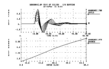
The ground bounce simulation presented duplicates Xilinx internal measurements methods; 8 to 32 outputs are simultaneously toggled. Each output is loaded with a 56-pF capacitance. The simulation uses an 84-pin package mode and an output buffer held at chip ground to measure the internal ground bounce.
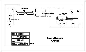
The simulation model is adjusted for the oscilloscope recordings for the two-bond wire ground.
qabounce.sp test of xilinx i/o buffers
* The following is the netlist for the above schematic(fig. 10-13)
.op
.option post list
.tran 1ns 50ns sweep gates 8 32 4
.measure bounce max v(out1x)
*.tran .1ns 7ns
.param gates=8
.print v(out1x) v(out8x) i(vdd) power
$.param xil_dtemp=-65 $ -40 degrees c (65 degrees from +25 degrees)
vdd vdd gnd 5.25
vgnd return gnd 0
upower1 vdd return iob1vdd iob1gnd pcb_power L=600mil
* local power supply capacitors
xc1a iob1vdd iob1gnd cap_mod cval=.1u
xc1b iob1vdd iob1gnd cap_mod cval=.1u
xc1c iob1vdd iob1gnd cap_mod cval=1u
xgnd_b iob1vdd iob1gnd out8x out1x xil_gnd_test
xcout8x out8x iob1gnd cap_mod m=gates
xcout1x out1x iob1gnd cap_mod m=1
.model pcb_power u LEVEL=3 elev=1 plev=1 nl=1 llev=1
+ th=1.3mil ht=10mil kd=4.5 dlev=1 wd=500mil xw=-2mil
.macro cap_mod node1 node2 cval=56p
Lr1 node1 node1x L=2nh R=0.05
cap node1x node2x c=cval
Lr2 node2x node2 L=2nh R=0.05
.eom
.macro xil_gnd_test vdd gnd outx outref
+ gates=8
* example of 8 iobuffers simultaneously switching
* through approx. 4nh lead inductance
* 1 iob is active low for ground bounce measurements
vout drive chipgnd pwl 0ns 5v, 10ns 5v, 10.5ns 0v,
$+ 20ns 0v, 20.5ns 5v, 40ns 5v R
x8 I8 drive PAD8x TS FAST PPUB TTL chipvdd chipgnd xil_iob
+ xil_sig=0 xil_dtemp=0 xil_shrink=1 M=gates
x1 I1 gnd PAD1x TS FAST PPUB TTL chipvdd chipgnd xil_iob
+ xil_sig=0 xil_dtemp=0 xil_shrink=1 m=1
rts ts chipgnd 1
rfast fast chipvdd 1
rppub ppub chipgnd 1
rttl ttl chipvdd 1
* pad model plcc84 rough estimates
lvdd vdd chipvdd L=3.0nh r=.02
lgnd gnd chipgnd L=3.0nh r=.02
lout8x outx pad8x L='5n/gates' r='0.05/gates'
lout1x outref pad1x L=5nh r=0.05
c_vdd_gnd chipvdd chipgnd 100n
.eom
.end
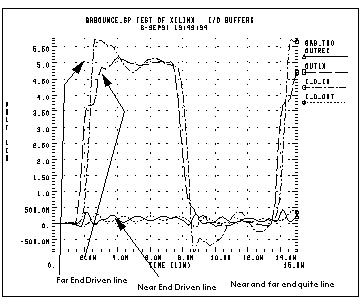
This example uses coupled noise to separate IOB parts. The output of one part drives the input of the other part through 0.6 inch of PCB. The example also monitors an adjacent quiet line.
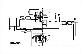
qa8.sp test of xilinx 0.8u i/o buffers
* The following is the netlist for the above schematic ( fig 10-15)
.op
.option nomod post=2
*.tran .1ns 5ns sweep xil_sig -3 3 3
.tran .1ns 15ns
.print v(out1x) v(out3x) i(vdd) v(irec)
vdd vdd gnd 5
vgnd return gnd 0
upower1 vdd return iob1vdd iob1gnd pcb_power L=600mil
upower2 vdd return iob2vdd iob2gnd pcb_power L=600mil
x4io iob1vdd iob1gnd out3x out1x outrec irec xil_iob4
cout3x out3x iob1gnd 9pf
u1x out1x outrec iob1gnd i_o_in i_o_out iob2gnd pcb_top L=2000mil
xrec iob2vdd iob2gnd i_o_in i_o_out xil_rec
.ic i_o_out 0v
.model pcb_top u LEVEL=3 elev=1 plev=1 nl=2 llev=1
+ th=1.3mil ht=10mil sp=5mil kd=4.5 dlev=1 wd=8mil xw=-2mil
.model pcb_power u LEVEL=3 elev=1 plev=1 nl=1 llev=1
+ th=1.3mil ht=10mil kd=4.5 dlev=1 wd=500mil xw=-2mil
.macro xil_rec vdd gnd tri1 tri2
* example of 2 iobuffers in tristate
xtri1 Irec O pad_tri1 TSrec FAST PPUB TTL chipvdd chipgnd xil_iob
+ xil_sig=0 xil_dtemp=0 xil_shrink=1 m=1
xtri2 Irec O pad_tri2 TSrec FAST PPUB TTL chipvdd chipgnd xil_iob
+ xil_sig=0 xil_dtemp=0 xil_shrink=1 m=1
rin_output O chipgnd 1
rtsrec tsrec chipvdd 1
rfast fast chipvdd 1
rppub ppub chipgnd 1
rttl ttl chipvdd 1
* pad model plcc84 rough estimates
lvdd vdd chipvdd L=1nh r=.01
lgnd gnd chipgnd L=1nh r=.01
ltri1 tri1 pad_tri1 L=3nh r=0.01
ltri2 tri2 pad_tri2 L=3nh r=.01
c_vdd_gnd chipvdd chipgnd 100n
.eom
.macro xil_iob4 vdd gnd out3x out1x outrec Irec
* example of 4 iobuffers simultaneously switching through approx.
* 3nh lead inductance
* 1 iob is a receiver (tristated)
vout O chipgnd pwl 0ns 0v, 1ns 0v, 1.25ns 4v, 7ns 4v, 7.25ns 0v, 12ns 0v R
x3 I3 O PAD3x TS FAST PPUB TTL chipvdd chipgnd xil_iob
+ xil_sig=0 xil_dtemp=0 xil_shrink=1 m=3
x1 I1 O PAD1x TS FAST PPUB TTL chipvdd chipgnd xil_iob
+ xil_sig=0 xil_dtemp=0 xil_shrink=1 m=1
xrec Irec O PADrec TSrec FAST PPUB TTL chipvdd chipgnd xil_iob
+ xil_sig=0 xil_dtemp=0 xil_shrink=1 m=1
* control settings
rts ts chipgnd 1
rtsrec tsrec chipvdd 1
rfast fast chipvdd 1
rppub ppub chipgnd 1
rttl ttl chipvdd 1
* pad model plcc84 rough estimates
lvdd vdd chipvdd L=1nh r=.01
lgnd gnd chipgnd L=1nh r=.01
lout3x out3x pad3x L=1nh r=.0033
lout1x out1x pad1x L=4nh r=0.01
loutrec outrec padrec L=4nh r=.01
c_vdd_gnd chipvdd chipgnd 100n
.eom
.end
* XILINX IOB INPUT/OUTPUT CIRCUIT
* NAME: XIL_IOB.INC
* PURPOSE: XILINX INPUT/OUTPUT BLOCK MODEL
* EXAMPLE OF CALL FOR 1.2U PART:
* X1 I O PAD TS FAST PPUB TTL VDD GND XIL_IOB
*+ XIL_SIG=0 XIL_DTEMP=0 XIL_SHRINK=0
* EXAMPLE OF CALL FOR 1.08U PART:
* X1 I O PAD TS FAST PPUB TTL VDD GND XIL_IOB
*+ XIL_SIG=0 XIL_DTEMP=0 XIL_SHRINK=1
*
* NAME: XIL_IOB.INC
* PURPOSE: XILINX INPUT/OUTPUT BLOCK MODEL
* PINS:
* I OUTPUT OF THE TTL/CMOS INPUT RECEIVER.
* O INPUT TO THE PAD DRIVER STAGE.
* PAD BONDING PAD CONNECTION.
* TS THREE-STATE CONTROL INPUT. HIGH LEVEL
* DISABLES PAD DRIVER.
* FAST SLEW RATE CONTROL. HIGH LEVEL SELECTS
* FAST SLEW RATE.
* PPUB PAD PULLL-UP ENABLE. ACTIVE LOW.
* TTL CMOS/TTL INPUT THRESHOLD SELECT. HIGH
* SELECTS TTL.
* VDD POSITIVE SUPPLY CONNECTION FOR INTERNAL
* CIRCUITRY.
* ALL THE ABOVE SIGNALS ARE REFERENCED TO NODE 0.
* THIS MODEL DOES CAUSE SOME DC CURRENT TO FLOW
* INTO NODE 0 THAT IS AN ARTIFACT OF THE MODEL.
* GND CIRCUIT GROUND
* THIS SUBCIRCUIT MODELS THE INTERFACE BETWEEN XILINX
* 3000 SERIES PARTS AND THE BONDING PAD. IT IS NOT
* USEFUL FOR PREDICTING DELAY TIMES FROM THE OUTSIDE
* WORLD TO INTERNAL LOGIC IN THE XILINX CHIP. RATHER,
* IT CAN BE USED TO PREDICT THE SHAPE OF WAVEFORMS
* GENERATED AT THE BONDING PAD AS WELL AS THE RESPONSE
* OF THE INPUT RECEIVERS TO APPLIED WAVEFORMS.
*
* THIS MODEL IS INTENDED FOR USE BY SYSTEM DESIGNERS
* WHO ARE CONCERNED ABOUT TRANSMISSION EFFECTS IN
* CIRCUIT BOARDS CONTAINING XILINX 3000 SERIES PARTS.
*
* THE PIN CAPACITANCE AND BONDING WIRE INDUCTANCE,
* RESISTANCE ARE NOT CONTAINED IN THIS MODEL. THESE
* ARE A FUNCTION OF THE CHOSEN PACKAGE AND MUST BE
* INCLUDED EXPLICITLY IN A CIRCUIT BUILT WITH THIS
* SUBCIRCUIT.
*
* NON-IDEALITIES SUCH AS GROUND BOUNCE ARE ALSO A
* FUNCTION OF THE SPECIFIC CONFIGURATION OF THE
* XILINX PART, SUCH AS THE NUMBER OF DRIVERS WHICH
* SHARE POWER PINS SWITCHING SIMULTANEOUSLY. ANY
* SIMULATION TO EXAMINE THESE EFFECTS MUST ADDRESS
* THE CONFIGURATION-SPECIFIC ASPECTS OF THE DESIGN.
*
.SUBCKT XIL_IOB I O PAD_IO TS FAST PPUB TTL VDD GND
+ XIL_SIG=0 XIL_DTEMP=0 XIL_SHRINK=1
.prot FREELIB
;]= $.[;qW.261DW3Eu0
VO\;:n[ $.[;qW.2'4%S+%X;:0[(3'1:67*8-:1:\[
kp39H2J9#Yo%XpVY#O!rDI$UqhmE%:\7%(3e%:\7\5O)1-5i# ;
.ENDS XIL_IOBStar-Hspice Manual - Release 2001.2 - June 2001