The Signetics I/O buffer library is distributed with Star-Hspice in the $installdir/parts/signet directory. These are high-performance parts used in backplane design. The transmission line model used describes two conductors.
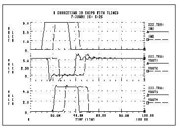
In the following application, a pair of drivers are driving about 2.5 inches of adjacent lines to a pair of receivers that drive about four inches of line.
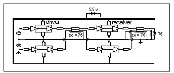
This is an example of connecting I/O chips with transmission lines.
.OPTIONS SEARCH='$installdir/parts/signet'
.OPTIONS POST=2 TNOM=27 NOMOD LIST METHOD=GEAR
.TEMP 27
$ DEFINE PARAMETER VALUES
.PARAM LV=0 HV=3 TD1=10n TR1=3n TF1=3n TPW=20n TPER=100n
+ TD2=20n TR2=2n TF2=2n LNGTH=101.6m
$ POWER SUPPLY
VCC VCC 0 DC 5.5
$ INPUT SOURCES
VIN1 STIM1 0 PULSE LV HV TD1 TR1 TF1 TPW TPER
VIN2 STIM2 0 PULSE LV HV TD2 TR2 TF2 TPW TPER
$ FIRST STAGE: DRIVER WITH TLINE
X1ST_TOP STIM1 OUTPIN1 VCC GND IO_CHIP PIN_IN=2.6n PIN_OUT=4.6n
X1ST_DN STIM2 OUTPIN2 VCC GND IO_CHIP PIN_IN=2.9n PIN_OUT=5.6n
U_1ST OUTPIN1 OUTPIN2 GND TLOUT1 TLOUT2 GND USTRIP L=LNGTH
$ SECOND STAGE: RECEIVER WITH TLINE
X2ST_TOP TLOUT1 OUTPIN3 VCC GND IO_CHIP PIN_IN=4.0n PIN_OUT=2.5n
X2ST_DN TLOUT2 OUTPIN4 VCC GND IO_CHIP PIN_IN=3.6n PIN_OUT=5.1n
U_2ST OUTPIN3 OUTPIN4 GND TLOUT3 TLOUT4 GND USTRIP L=LNGTH
$ TERMINATING RESISTORS
R1 TLOUT3 GND 75
R2 TLOUT4 GND 75
$ IO CHIP MODEL - SIGNETICS
.SUBCKT IO_CHIP IN OUT VCC XGND PIN_VCC=7n PIN_GND=1.8n
X1 IN1 INVOUT VCC1 XGND1 ACTINPUT
X2 INVOUT OUT1 VCC1 XGND1 AC109EQ
LIN_PIN IN IN1 PIN_IN
LOUT_PIN OUT1 OUT PIN_OUT
LVCC VCC VCC1 PIN_VCC
LGND XGND1 XGND PIN_GND
.ENDS
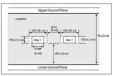
$ TLINE MODEL - 2 SIGNAL CONDUCTORS WITH GND
$ PLANE
.MODEL USTRIP U LEVEL=3 ELEV=1 PLEV=1
+ TH1=1.3mil HT1=10mil TS=32mil KD1=4.5 DLEV=0 WD1=8mil
+ XW=-2mil KD2=4.5 NL=2 SP12=5mil
$ ANALYSIS / PRINTS
.TRAN .1NS 100NS
.GRAPH IN1=V(STIM1) IN2=V(STIM2) VOUT1=V(TLOUT1) VOUT2=V(TLOUT2)
.GRAPH VOUT3=V(TLOUT3) VOUT4=V(TLOUT4)
.END