


To simulate a PC board or backplane with Star-Hspice, you must consider models for:
It is important to model the transmission line as closely as possible-- that is, to include all electrical elements exactly as they are laid out on the backplane or printed circuit board, to maintain the integrity of the simulation.
With readily available I/O drivers from ASIC vendors and Star-Hspice's advanced lossy transmission lines, you can simulate the electrical behavior of the board interconnect, bus, or backplane to analyze the transmission line behavior under various conditions.
Simulation is possible because the critical models and simulation technology exist.
Star-Hspice has been enhanced for systems simulation with:
The following vendor models are currently available in Star-Hspice:
Some signal integrity problems that can cause failures in high-speed designs are listed in High-Speed Design Problems and Solutions.
Circuit simulation of a digital system only becomes necessary when the analog characteristics of the digital signals become electrically important. Is the digital circuit a new design, or simply a fast version of the old design? Many new digital products are really faster versions of existing designs. The transition from a 100 MHz to a 150 MHz Pentium PC may not require extensive logic simulations. However, the integrity of the digital quality of the signals may require very careful circuit analysis.
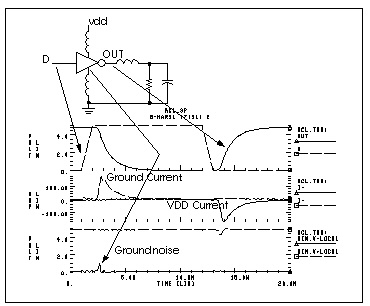
The source of a signal integrity problem is the digital output driver. A high-speed digital output driver can only drive a few inches before the noise and delay due to the wiring become a problem. To speed up circuit simulation and modeling, you can create analog behavioral models that mimic the full analog characteristics at a fraction of the traditional evaluation time. The simulation of the output buffer in Simulation of Output Buffer with 2 ns Delay and 1.8 ns Rise and Fall Times demonstrates the analog behavior of a digital gate simulated in the Star-Hspice circuit simulator.
The roadblocks to successful high-speed digital designs are noise and signal delays. Digital noise can come from several sources. The fundamental digital noise sources are:
Line termination noise is the additional voltage that is reflected from the load back to the driver because of impedance mismatch. Digital output buffers are not designed to have accurately controlled output impedance and most buffers have different rising and falling edge impedances.
Ground bounce noise is generated where leadframes or other circuit wires cannot be formed into transmission lines. The resulting inductance creates an induced voltage in the ground circuit, the supply circuit, and the output driver circuit. The ground bounce noise lowers the noise margins for the rest of the system. Coupled line noise is the noise induced from lines that are physically adjacent. This noise is generally most severe for data lines that are next to clock lines.
Circuit delays become critical as timing requirements become tighter. The key circuit delays are:
Logic analysis only addresses gate delays. You can compute the variation in the gate delay from circuit simulation only if you understand the best case and worst case manufacturing conditions. The line turnaround delays add to the gate delays because extra margin must be added so that multiple tristate buffer drivers do not simultaneously turn on. The line length delay affects the clock skew most directly in most systems. As system cycle times approach the speed of electromagnetic signal propagation for the printed circuit board, consideration of the line length becomes critical. The system noises and line delays interact with the electrical characteristics of the gates and may require circuit level simulation.
Analog details find digital systems problems. Exceeding the noise quota may not cause a system to fail. Only when a digital input is being accepted does the maximum noise become a problem. If a digital systems engineer can decouple the system, much higher noise can be accepted.
Common decoupling methods are:
In present systems designs, you must select the best packaging methods at the printed circuit board level, the multi-chip module level, and the pin grid array level. Extra ground and power planes are often necessary to lower the supply inductance and provide decoupling. Decoupling capacitors must have very low internal inductance in order to be effective for high speed designs. Newer designs frequently use series resistance in the output drivers to lower circuit ringing. Finally, in critical high speed driver applications, twisted differential pair transmission lines are used.
The systems engineer must determine how to partition the logic. The propagation speed of signals on a printed circuit board is about 6 in/ns. As digital designs become faster, the wiring interconnect becomes a factor in deciding how to partition the logic. The critical wiring systems are:
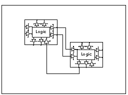
Systems designers who use ASIC or custom integrated circuits as part of their system logic partitioning strategy find that they must make decisions about integrated circuit level wiring. The more familiar decisions involve the selection of packages and the arrangement of packages on a printed circuit board. Large systems generally have a central backplane that becomes the primary challenge at the system partition level.
Use the following equation to estimate wire length when transmission line effects become noticeable:
critical length=(rise time)*velocity/8
For example, if rise time is 1 ns and board velocity is 6 in/ns, distortion becomes noticeable at a wire length of 3/4 in. The Star-Hspice circuit simulator automatically generates models for each type of wire to define full loss transmission line effects.
ECL logic design engineers typically partitioned the system by calculating the noise quota for each line. Now, most high-speed digital logic must be designed with respect to the noise quota so that the engineer knows how much noise and delay can be accepted before the timing and logic levels fail.
To solve the noise quota problem, you must calculate the noise associated with the wiring. Large integrated circuits can be separated into two parts: the internal logic and the external input and output amplifiers.
Using mixed digital and analog tools such as Avant!'s Star-Hspice and Viewlogic's Viewsim A/D, you can merge a complete system together with full analog quality timing constraints and full digital representation. You can simultaneously evaluate noise quota calculation subject to system timing.
Star-Hspice Manual - Release 2001.2 - June 2001