LEVEL 61 RPI a-Si TFT Model
Star-Hspice LEVEL 61 is an AIM-SPICE MOS15 amorphous silicon (a-Si) thin-film transistor (TFT) model.
Model Features
AIM-SPICE MOS15 a-Si TFT model features include:
-
Modified charge control model; induced charge trapped in localized states
-
Above threshold includes:
-
Field effect mobility becoming a function of gate bias
-
Band mobility dominated by lattice scattering
-
Below threshold
-
Fermi level located in deep localized states
-
Relate position of Fermi level, including the deep DOS back to the gate bias
-
Empirical expression for current at large negative gate biases for hole-induced leakage current
-
Interpolation techniques are applied to the equations to unify the model
Using LEVEL 61 with Star-Hspice
When using the AIM-SPICE MOS15 a-Si TFT model:
1. Set LEVEL=61 to identify the model as the AIM-SPCIE MOS15 a-Si TFT model.
2. The default value for L is 100m, and the default value for W is 100m.
3. The LEVEL 61 model is a 3-terminal model. No bulk node exists; therefore no parasitic drain-bulk or source-build diodes are appended to the model. A fourth node can be specified, but does not affect simulation results.
4. The default room temperature is 25C in Star-Hspice, but is 27C in some other simulators. The user may choose whether or not to set the nominal simulation temperature to 27C, by adding .OPTION TNOM=27 to the netlist.
Example
This is an example of how the Star-Hspice model and element statement modified for use with LEVEL 61.
mckt drain gate source nch L=10e-6 W=10e-6
.MODEL nch nmos LEVEL=61
+ alphasat = 0.6 cgdo = 0.0 cgso = 0.0 def0 = 0.6
+ delta = 5.0 el = 0.35 emu = 0.06 eps = 11
+ epsi = 7.4 gamma = 0.4 gmin = 1e23 iol = 3e-14
+ kasat = 0.006 kvt = -0.036 lambda = 0.0008 m = 2.5
+ muband = 0.001 rd = 0.0 rs = 0.0 sima0 = 1e-14
+ tnom = 27 tox = 1.0e-7 v0 = 0.12 vaa = 7.5e3
+ vdsl = 7 vfb = -3 vgsl = 7 vmin = 0.3 vto = 0.0
LEVEL 61 Model Parameters
|
Name
|
Unit
|
Default
|
Description
|
|
ALPHASAT
|
-
|
0.6
|
Saturation modulation parameter
|
|
CGDO
|
F/m
|
0.0
|
Gate-drain overlap capacitance per meter channel width
|
|
CGSO
|
F/m
|
0.0
|
Gate-source overlap capacitance per meter channel width
|
|
DEF0
|
eV
|
0.6
|
Dark Fermi level position
|
|
DELTA
|
-
|
5
|
Transition width parameter
|
|
EL
|
eV
|
0.35
|
Activation energy of the hole leakage current
|
|
EMU
|
eV
|
0.06
|
Field effect mobility activation energy
|
|
EPS
|
-
|
11
|
Relative dielectric constant of substrate
|
|
EPSI
|
-
|
7.4
|
Relative dielectric constant of gate insulator
|
|
GAMMA
|
-
|
0.4
|
Power law mobility parameter
|
|
GMIN
|
m-3eV-1
|
1E23
|
Minimum density of deep states
|
|
IOL
|
A
|
3E-14
|
Zero bias leakage current parameter
|
|
KASAT
|
1/°
C
|
0.006
|
Temperature coefficient of ALPHASAT
|
|
KVT
|
V/°
C
|
-0.036
|
Threshold voltage temperature coefficient
|
|
LAMBDA
|
1/V
|
0.0008
|
Output conductance parameter
|
|
M
|
-
|
2.5
|
Knee shape parameter
|
|
MUBAND
|
m2/Vs
|
0.001
|
Conduction band mobility
|
|
RD
|
µ
|
0.0
|
Drain resistance
|
|
RS
|
µ
|
0.0
|
Source resistance
|
|
SIGMA0
|
A
|
1E-14
|
Minimum leakage current parameter
|
|
TNOM
|
oC
|
25
|
Parameter measurement temperature
|
|
TOX
|
m
|
1E-7
|
Thin-oxide thickness
|
|
V0
|
V
|
0.12
|
Characteristic voltage for deep states
|
|
VAA
|
V
|
7.5E3
|
Characteristic voltage for field effect mobility
|
|
VDSL
|
V
|
7
|
Hole leakage current drain voltage parameter
|
|
VFB
|
V
|
-3
|
Flat band voltage
|
|
VGSL
|
V
|
7
|
Hole leakage current gate voltage parameter
|
|
VMIN
|
V
|
0.3
|
Convergence parameter
|
|
VTO
|
V
|
0.0
|
Zero-bias threshold voltage
|
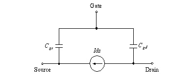
Equivalent Circuit
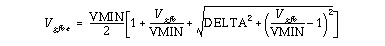
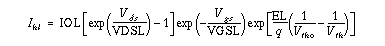
Model Equations
Drain Current
Temperature Dependence
Capacitance
Star-Hspice Manual - Release 2001.2 - June 2001