LEVEL 62 RPI Poli-Si TFT Model
Star-Hspice LEVEL 62 is an AIM-SPICE MOS16 poly-silicon (Poli-Si) thin-film transistor (TFT) model.
Model Features
The AIM-SPICE MOS16 Poli-Si TFT model features include:
-
A design based on the crystalline MOSFET model
-
Field effect mobility that becomes a function of gate bias
-
Effective mobility that accounts for trap states:
-
For low V
gs
, it is power law
-
For high V
gs
, it is constant
-
Reverse bias drain current function of electric field near drain and temperature
-
A design independent of channel length
-
A unified DC model that includes all four regimes for channel lengths down to 4 m:
-
Leakage (thermionic emission)
-
Subthreshold (diffusion-like model)
-
Above threshold (c-Si-like, with mFet)
-
Kink (impact ionization with feedback)
-
An AC model that accurately reproduces C
gc
frequency dispersion
-
An automatic scaling of model parameters that accurately model a wide range of device geometries
Using LEVEL 62 with Star-Hspice
When using the AIM-SPICE MOS16 Poli-Si TFT model:
1. Set LEVEL=62 to identify the model as the AIM-SPICE MOS16 Poli-Si TFT model.
2. The default value for L is 100m, and the default value for W is 100m.
3. The LEVEL 62 model is a 3-terminal model. No bulk node exists; therefore no parasitic drain-bulk or source-bulk diodes are appended to the model. A fourth node can be specified, but does not affect simulation results.
4. The default room temperature is 25oC in Star-Hspice, but is 27oC in some other simulators. The user may choose whether or not to set the nominal simulation temperature to 27oC by adding .OPTION TNOM=27 to the netlist.
Example
This is an example of a Star-Hspice model and element statement modified for use with LEVEL 62:
mckt drain gate source nch L=10e-6 W=10e-6
.MODEL nch nmos LEVEL=62
+ asat = 1 at = 3e-8 blk = 0.001 bt = 0.0 cgdo = 0.0
+ cgso = 0.0 dasat = 0.0 dd = 1.4e-7 delta = 4.0
+ dg = 2.0e-7 dmu1 = 0.0 dvt = 0.0 dvto = 0.0 eb = 0.68
+ eta = 7 etac0 = 7 etac00 = 0 i0 = 6.0 i00 = 150
+ lasat = 0lkink = 19e-6 mc = 3.0 mk = 1.3 mmu = 3.0
+ mu0 = 100 mu1 = 0.0022 mus = 1.0 rd = 0.0 rdx = 0.0
+ rs = 0.0 rsx = 0.0 tnom = 27 tox = 1.0e=7 vfb = -0.1
+ vkink = 9.1 von = 0.0 vto = 0.0
LEVEL 62 Model Parameters
|
Name
|
Unit
|
Default
|
Description
|
|
ASAT
|
-
|
1
|
Proportionality constant of Vsat
|
|
AT
|
m/V
|
3E-8
|
DIBL parameter 1
|
|
BLK
|
-
|
0.001
|
Leakage barrier lowering constant
|
|
BT
|
m.V
|
1.9E-6
|
DIBL parameter 2
|
|
CGDO
|
F/m
|
0
|
Gate-drain overlap capacitance per meter channel width
|
|
CGSO
|
F/m
|
0
|
Gate-source overlap capacitance per meter channel width
|
|
DASAT
|
1/°C
|
0
|
Temperature coefficient of ASAT
|
|
DD
|
m
|
1400 Å
|
Vds field constant
|
|
DELTA
|
-
|
4.0
|
Transition width parameter
|
|
DG
|
m
|
2000 Å
|
Vgs field constant
|
|
DMU1
|
cm2/Vs
°
C
|
0
|
Temperature coefficient of MU1
|
|
DVT
|
V
|
0
|
The difference between VON and the threshold voltage
|
|
DVTO
|
V/°C
|
0
|
Temperature coefficient of VTO
|
|
EB
|
EV
|
0.68
|
Barrier height of diode
|
|
ETA
|
-
|
7
|
Subthreshold ideality factor
|
|
ETAC0
|
-
|
ETA
|
Capacitance subthreshold ideality factor at zero drain bias
|
|
ETAC00
|
1/V
|
0
|
Capacitance subthreshold coefficient of drain bias
|
|
I0
|
A/m
|
6.0
|
Leakage scaling constant
|
|
I00
|
A/m
|
150
|
Reverse diode saturation current
|
|
LASAT
|
M
|
0
|
Coefficient for length dependence of ASAT
|
|
LKINK
|
M
|
19E-6
|
Kink effect constant
|
|
MC
|
-
|
3.0
|
Capacitance knee shape parameter
|
|
MK
|
-
|
1.3
|
Kink effect exponent
|
|
MMU
|
-
|
3.0
|
Low field mobility exponent
|
|
MU0
|
cm2/Vs
|
100
|
High field mobility
|
|
MU1
|
cm2/Vs
|
0.0022
|
Low field mobility parameter
|
|
MUS
|
cm2/Vs
|
1.0
|
Subthreshold mobility
|
|
RD
|
µ
|
0
|
Drain resistance
|
|
RDX
|

|
0
|
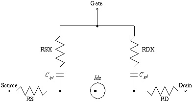
Resistance in series with Cgd
|
|
RS
|
µ
|
0
|
Source resistance
|
|
RSX
|

|
0
|
Resistance in series with Cgs
|
|
TNOM
|
°C
|
25
|
Parameter measurement temperature
|
|
TOX
|
m
|
1e-7
|
Thin-oxide thickness
|
|
V0
|
V
|
0.12
|
Characteristic voltage for deep states
|
|
VFB
|
V
|
-0.1
|
Flat band voltage
|
|
VKINK
|
V
|
9.1
|
Kink effect voltage
|
|
VON
|
V
|
0
|
On-voltage
|
|
VTO
|
V
|
0
|
Zero-bias threshold voltage
|
Equivalent Circuit
Model Equations
Drain Current
The expression for the subthreshold current is given by:
where  is the dielectric constant of the oxide and k
B
is the Boltzmanns constant.
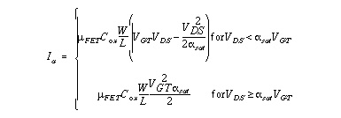
Above threshold (
Vgt
> 0), the conduction current is given by:
Subthreshold leakage current is the result of thermionic field emission of carriers through the grain boundary trap states and is described by:
Finally, for very large drain biases, the kink effect is observed. It is modeled as impact ionization in a narrow region near the drain. The expression can be written as:
The impact ionization current,
Ikink
, is added to the drain current.
Threshold Voltage
If VTO is not specified:
else:
Temperature Dependence
Capacitance
U
Star-Hspice Manual - Release 2001.2 - June 2001


 is the dielectric constant of the oxide and k


