|
Mxxx
|
SOI MOSFET element name. Must begin with M, which can be followed by up to 1023 alphanumeric characters
|
|
nd
|
Drain terminal node name or number
|
|
ng
|
Front gate node name or number
|
|
ns
|
Source terminal node name or number
|
|
ne
|
Back gate (or Substrate) node name or number
|
|
np
|
External body contact node name or number
|
|
mname
|
MOSFET model name reference
|
|
L
|
SOI MOSFET channel length in meters. This parameter overrides DEFL in an OPTIONS statement
Default=DEFL with a maximum of 0.1m
|
|
W
|
SOI MOSFET channel width in meters. This parameter overrides DEFW in an OPTIONS statement
Default=DEFW with a maximum of 0.1m
|
|
M
|
Multiplier to simulate multiple SOI MOSFETs in parallel. All channel widths, diode leakages, capacitances and resistances are affected by the setting of M
Default=1
|
|
AD
|
Drain diffusion area. Overrides DEFAD in the OPTIONS statement
Default=DEFAD
|
|
AS
|
Source diffusion area. Overrides DEFAS in the OPTIONS statement
Default=DEFAS
|
|
PD
|
Perimeter of the drain junction, including the channel edge. Overrides DEFPD in the OPTIONS statement
|
|
PS
|
Perimeter of the source junction, including the channel edge. Overrides DEFPS in the OPTIONS statement
|
|
NRD
|
Number of squares of drain diffusion for drain series resistance. Overrides DEFNRD in the OPTIONS statement
|
|
NRS
|
Number of squares of source diffusion for source series resistance. Overrides DEFNRS in the OPTIONS statement
|
|
NRB
|
Number of squares for body series resistance
|
|
RDC
|
Additional drain resistance due to contact resistance with units of ohms. This value overrides the RDC setting in the model specification
Default =0.0
|
|
RSC
|
Additional source resistance due to contact resistance with units of ohms. This value overrides the RDC setting in the model specification
Default=0.0
|
|
RTHO
|
Thermal resistance per unit width
-
If not specified, RTHO is extracted from the model card
-
If specified, it will override the one in the model card
|
|
CTHO
|
Thermal capacitance per unit width
-
If not specified, CTHO is extracted from the model card
-
If specified, it will override the one in the model card
|
|
OFF
|
Sets initial condition to OFF for this element in DC analysis
|
|
BJTOFF
|
Turns off BJT if equal to 1
|
|
IC
|
Initial guess in the order (drain, front gate, internal body, back gate, external voltage). Vps will be ignored in the case of 4-terminal device. These are used when UIC is present in the .TRAN statement and are overriden by the .IC statement
|
DC Parameters
|
SPICE
Symbol
|
Description
|
Unit
|
Default
|
Notes (below)
|
|
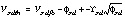
vth0
|
Threshold voltage @ V
bs
=0 for long and wide device
|
-
|
0.7
|
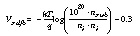
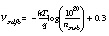
nI-3
|
|
k1
|
First order body effect coefficient
|
V
1/2
|
0.6
|
-
|
|
k2
|
Second order body effect coefficient
|
-
|
0
|
-
|
|
k3
|
Narrow width coefficient
|
-
|
0
|
-
|
|
k3b
|
Body efficient coefficent of k3
|
1/V
|
0
|
-
|
|
Vbsa
|
Transition body voltage offset
|
V
|
0
|
-
|
|
delp
|
Constant for limiting Vbseff to φs
|
V
|
0.02
|
-
|
|
Kb1
|
Coefficient of Vbs0 dependency on Ves
|
-
|
1
|
-
|
|
Kb3
|
Coefficient of Vbs0 dependency on V
gs
at subthreshold region
|
-
|
1
|
-
|
|
Dvbd0
|
First coefficient of Vbs0 dependency on Leff
|
V
|
0
|
-
|
|
Dvbd1
|
Second coefficient of Vbs0 dependency on Leff
|
V
|
0
|
-
|
|
w0
|
Narrow width parameter
|
m
|
0
|
-
|
|
nlx
|
Lateral non-uniform doping parameter
|
m
|
1.74e-7
|
-
|
|
dvt0
|
First coefficient of short-channel effect on Vth
|
-
|
2.2
|
-
|
|
dvt1
|
Second coefficient of short-channel effect on Vth
|
-
|
0.53
|
-
|
|
dvt2
|
Body-bias coefficient of short-channel effect on Vth
|
1/V
|
-0.032
|
-
|
|
dvt0w
|
First coefficient of narrow width effect on Vth for small channel length
|
-
|
0
|
-
|
|
dvt1w
|
Second coefficient of narrow width effect on Vth for small channel length
|
-
|
5.3e6
|
-
|
|
dvt2w
|
Body-bias coefficient of narrow width effect on Vth for small channel length
|
1/V
|
-0.032
|
-
|
|
u0
|
Mobility at Temp = Tnom
NMOSFET
PMOSFET
|
cm
2
/(V-sec)
|
670
250
|
-
|
|
ua
|
First-order mobility degradation coefficient
|
m/V
|
2.25e-9
|
-
|
|
ub
|
Second-order mobility degradation coefficient
|
(m/V)
2
|
5.9e-19
|
-
|
|
uc
|
Body-effect of mobility degradation coefficient
|
1/V
|
-.0465
|
-
|
|
vsat
|
Saturation velocity at Temp = Tnom
|
m/sec
|
8e4
|
-
|
|
a0
|
Bulk charge effect coefficient for channel length
|
-
|
1.0
|
-
|
|
ags
|
Gate bias coefficient of A
bulk
|
1/V
|
0.0
|
-
|
|
b0
|
Bulk charge effect coefficient for channel width
|
m
|
0.0
|
-
|
|
b1
|
Bulk charge effect width offset
|
m
|
0.0
|
-
|
|
keta
|
Body-bias coefficient of bulk charge effect
|
m
|
-0.6
|
-
|
|
Abp
|
Coefficient of Abeff dependency on Vgst
|
-
|
1.0
|
-
|
|
mxc
|
Fitting parameter for Abeff calculation
|
-
|
-0.9
|
-
|
|
adice0
|
DICE bulk charge factor
|
-
|
1
|
-
|
|
A1
|
First non-saturation effect parameter
|
1/V
|
0.0
|
-
|
|
A2
|
Second non-saturation effect parameter
|
0
|
1.0
|
-
|
|
rdsw
|
Parasitic resistance per unit width
|
Ω
−µm
Wr
|
100
|
-
|
|
prwb
|
Body effect coefficient Rdsw
|
1/V
|
0
|
-
|
|
prwg
|
Gate bias effect coefficient of Rdsw
|
1/V
1/2
|
0
|
-
|
|
wr
|
Width offset from Weff for Rds calculation
|
-
|
1
|
-
|
|
wint
|
Width offset fitting parameter from I-V without bias
|
m
|
0.0
|
-
|
|
lint
|
Length offset fitting parameter from I-V without bias
|
m
|
0.0
|
-
|
|
dwg
|
Coefficient of W
eff
's gate dependence
|
m/V
|
0.0
|
|
|
dwb
|
Coefficient of W
eff
's substrate body bias dependence
|
m/V
1/2
|
0.0
|
|
|
voff
|
Offset voltage in the subthreshold region for large W and L
|
V
|
-0.08
|
-
|
|
nfactor
|
Subthreshold swing factor
|
-
|
1
|
-
|
|
eta0
|
DIBL coefficient in subthreshold region
|
-
|
0.08
|
-
|
|
etab
|
Body-bias coefficient for the subthreshold DIBL effect
|
1/V
|
-0.07
|
-
|
|
dsub
|
DIBL coefficient exponent
|
-
|
0.56
|
-
|
|
cit
|
Interface trap capacitance
|
F/m
2
|
0.0
|
-
|
|
cdsc
|
Drain/Source to channel coupling capacitance
|
F/m
2
|
2.4e-4
|
-
|
|
cdscb
|
Body-bias sensitivity of C
dsc
|
F/m
2
|
0
|
-
|
|
cdscd
|
Drain-bias sensitivity of C
dsc
|
F/m
2
|
0
|
-
|
|
pclm
|
Channel length modulation parameter
|
-
|
1.3
|
-
|
|
pdibl1
|
First output resistance DIBL effect correction parameter
|
-
|
.39
|
-
|
|
pdibl2
|
Second output resistance DIBL effect correction parameter
|
-
|
0.086
|
-
|
|
drout
|
L dependence coefficient of the DIBL correction parameter in Rout
|
-
|
0.56
|
-
|
|
pvag
|
Gate dependence of early voltage
|
-
|
0.0
|
-
|
|
delta
|
Effective V
ds
parameter
|
-
|
0.01
|
-
|
|
aii
|
1st Leff dependence Vdsatii parameter
|
1/V
|
0.0
|
-
|
|
bii
|
2nd Leff dependence Vdsatii parameter
|
m/V
|
0.0
|
-
|
|
cii
|
1st Vds dependence Vdsatii parameter
|
-
|
0.0
|
-
|
|
dii
|
2nd dependence Vdsatii parameter
|
V
|
-1.0
|
-
|
|
alpha0
|
First parameter of impact ionization current
|
m/V
|
0.0
|
-
|
|
alpha1
|
Second parameter of impact ionization current
|
1/V
|
1.0
|
-
|
|
beta0
|
Third parameter of impact ionization current
|
V
|
30
|
-
|
|
Agidl
|
GIDL constant
|
Ω-1
|
0.0
|
-
|
|
Bgidl
|
GIDL exponential coefficient
|
V/m
|
0.0
|
-
|
|
Ngidl
|
GIDL Vds enhancement coefficient
|
V
|
1.2
|
-
|
|
ntun
|
Reverse tunneling non-ideality factor
|
-
|
10.0
|
-
|
|
Ndiode
|
Diode non-ideality factor
|
-
|
1.0
|
-
|
|
Isbjt
|
BJT injection saturation current
|
A/m2
|
1e-6
|
-
|
|
Isdif
|
Body to source/drain injection saturation current
|
A/m2
|
0.0
|
-
|
|
Isrec
|
Recombination in depletion saturation current
|
A/m2
|
1e-5
|
-
|
|
Istun
|
Reverse tunneling saturation current
|
A/m2
|
0.0
|
-
|
|
Edl
|
Electron diffusion length
|
m
|
2e-6
|
-
|
|
Kbjt1
|
Parasitic bipolar early effect coefficient
|
m/V
|
0
|
-
|
|
Rbody
|
Intrinsic body contact sheet resistance
|
ohm/m2
|
0.0
|
-
|
|
Rbsh
|
Extrinsic body contact sheet resistance
|
ohm/m2
|
0.0
|
-
|
|
rsh
|
Source drain sheet resistance in ohm per square
|
Ω
/squre
|
0.0
|
-
|
AC and Capacitance Parameters
|
SPICE
Symbol
|
Description
|
Unit
|
Default
|
Notes (below)
|
|
xpart
|
Charge partitioning rate flag
|
-
|
0
|
|
|
cgso
|
Non LDD region source-gate overlap capacitance per channel length
|
F/m
|
calcu-
lated
|
nC-1
|
|
cgdo
|
Non LDD region drain-gate overlap capacitance per channel length
|
F/m
|
calcu-
lated
|
nC-2
|
|
cgeo
|
Gate substrate overlap capacitance per unit channel length
|
F/m
|
0.0
|
-
|
|
cjswg
|
Source/Drain (gate side) sidewall junction
Capacitance per unit width (normalized to 100nm T
si
)
|
F/m
2
|
1e-10
|
-
|
|
pbswg
|
Source/Drain (gate side) sidewall junction capacitance built in potential
|
V
|
.7
|
-
|
|
mjswg
|
Source/Drain (gate side) sidewall junction capacitance grading coefficient
|
V
|
0.5
|
-
|
|
tt
|
Diffusion capacitance transit time coefficient
|
second
|
1ps
|
-
|
|
vsdfb
|
Source/drain bottom diffusion capacitance flatband voltage
|
V
|
calcu-
lated
|
nC-3
|
|
vsdth
|
Source/drain bottom diffusion capacitance threshold voltage
|
V
|
calcu-
lated
|
nC-4
|
|
csdmin
|
Source/drain bottom diffusion minimum capacitance
|
V
|
calcu-
lated
|
nC-5
|
|
asd
|
Source/drain bottom diffusion smoothing parameter
|
-
|
0.3
|
-
|
|
csdesw
|
Source/drain sidewall fringing capacitance per unit length
|
F/m
|
0.0
|
-
|
|
cgs1
|
Light doped source-gate region overlap capacitance
|
F/m
|
0.0
|
-
|
|
cgd1
|
Light doped drain-gate region overlap capacitance
|
F/m
|
0.0
|
-
|
|
ckappa
|
Coefficient for lightly doped region overlap capacitance fringing field capacitance
|
F/m
|
0.6
|
-
|
|
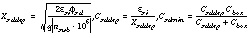
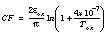
cf
|
Gate to source/drain fringing field capacitance
|
F/m
|
calcu-
lated
|
nC-6
|
|
clc
|
Constant term for the short channel mode
|
m
|
0.1x10
-7
|
-
|
|
cle
|
Exponential term for the short channel mode
|
none
|
0.0
|
-
|
|
dlc
|
Length offset fitting parameter from C-V
|
m
|
lint
|
-
|
|
dwc
|
Width offset fitting parameter from C-V
|
m
|
wint
|
-
|
Temperature Parameters
|
SPICE
Symbol
|
Description
|
Unit
|
Default
|
Notes (below)
|
|
tnom
|
Temperature at which parameters are expected
|
o
C
|
27
|
-
|
|
ute
|
Mobility temperature exponent
|
none
|
-1.5
|
-
|
|
kt1
|
Temperature coefficient for threshold voltage
|
V
|
-0.11
|
-
|
|
kt11
|
Channel length dependence of the temperature coefficient for threshold voltage
|
V*m
|
0.0
|
|
|
kt2
|
Body-bias coefficient of the Vth temperature effect
|
none
|
0.022
|
-
|
|
ua1
|
Temperature coefficient for U
a
|
m/V
|
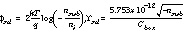
4.31e-9
|
-
|
|
ub1
|
Temperature coefficient for U
b
|
(m/V)
2
|
-7.61e-18
|
-
|
|
uc1
|
Temperature coefficient for U
c
|
1/V
|
-.056
|
nT-1
|
|
at
|
Temperature coefficient for saturation velocity
|
m/sec
|
3.3e4
|
-
|
|
cth0
|
Normalized thermal capacity
|
moC/(W*sec)
|
0
|
-
|
|
prt
|
Temperature coefficient for Rdsw
|
Ω
-
µ
m
|
0
|
-
|
|
rth0
|
Normalized thermal resistance
|
moC/W
|
0
|
-
|
|
xbjt
|
Power dependence of jbjt on temperature
|
none
|
2
|
-
|
|
xdif
|
Power dependence of jdif on temperature
|
none
|
2
|
-
|
|
xrec
|
Power dependence of jrec on temperature
|
none
|
20
|
-
|
|
xtun
|
Power dependence of j
tun
on temperature
|
none
|
0
|
-
|