|
Mxxx
|
SOI MOSFET element name. Must begin with M, which can be followed by up to 1023 alphanumeric characters.
|
|
nd
|
Drain terminal node name or number
|
|
ng
|
Front gate node name or number
|
|
ns
|
Source terminal node name or number
|
|
ne
|
Back gate (or substrate) node name or number
|
|
np
|
Optional external body contact node name or number
|
|
mname
|
MOSFET model name reference
|
|
L
|
SOI MOSFET channel length in meters. This parameter overrides DEFL in an OPTIONS statement. Default=DEFL with a maximum of 0.1m.
|
|
W
|
MOSFET channel width in meters. This parameter overrides DEFW in an OPTIONS statement. Default=DEFW.
|
|
M
|
Multiplier to simulate multiple SOI MOSFETs in parallel. All channel widths, diode leakages, capacitances and resistances are affected by the setting of M. Default=1.
|
|
AD
|
Drain diffusion area. Overrides DEFAD in the OPTIONS statement. Default=DEFAD.
|
|
AS
|
Source diffusion area. Overrides DEFAS in the OPTIONS statement. Default=DEFAS.
|
|
PD
|
Perimeter of the drain junction, including the channel edge. Overrides DEFPD in the OPTIONS statement.
|
|
PS
|
Perimeter of the source junction, including the channel edge. Overrides DEFPS in the OPTIONS statement.
|
|
NRD
|
Number of squares of drain diffusion for drain series resistance. Overrides DEFNRD in the OPTIONS statement.
|
|
NRS
|
Number of squares of source diffusion for source series resistance. Overrides DEFNRS in the OPTIONS statement.
|
|
NRB
|
Number of squares for body series resistance.
|
|
RTH0
|
Thermal resistance per unit width
-
If not specified, RTH0 is extracted from the model card.
-
If specified, it overrides the one in the model card.
|
|
CTH0
|
Thermal capacitance per unit width
-
If not specified, CTH0 is extracted from model card.
-
If specified, it overrides the one in the model card.
|
|
OFF
|
Sets initial condition to OFF for this element in DC analysis
|
|
BJTOFF
|
Turning off BJT if equal to 1
|
|
IC
|
Initial guess in the order (drain, front gate, internal body, back gate, external voltage). (Vps is ignored in the case of 4-terminal device) These are used when UIC is present in the .TRAN statement and are overridden by the .IC statement.
|
|
Parameter
|
Unit
|
Default
|
Description
|
|
A0
|
-
|
1.0
|
Bulk charge effect coefficient for channel length
|
|
A1
|
1/V
|
0.0
|
First non-saturation effect parameter
|
|
A2
|
-
|
1.0
|
Second non-saturation effect parameter
|
|
ABP
|
-
|
1.0
|
Coefficient of Abeff dependency on
Vgst
|
|
ADICE0
|
-
|
1
|
DICE bulk charge factor
|
|
AGIDL
|
1/W
|
0.0
|
GIDL constant
|
|
AGS
|
1/V
|
0.0
|
Gate bias coefficient of Abulk
|
|
AII
|
1/V
|
0.0
|
First Leff dependence Vdsatii parameter
|
|
ALPHA0
|
m/V
|
0.0
|
The first parameter of impact ionization current
|
|
ALPHA1
|
1/V
|
1.0
|
The second parameter of impact ionization current
|
|
B0
|
m
|
0.0
|
Bulk charge effect coefficient for channel width
|
|
B1
|
m
|
0.0
|
Bulk charge effect width offset
|
|
BGIDL
|
V/m
|
0.0
|
GIDL exponential coefficient
|
|
BII
|
m/V
|
0.0
|
Second Leff dependence Vdsatii parameter
|
|
CDSC
|
F/m2
|
2.4e-4
|
Drain/source to channel coupling capacitance
|
|
CDSCB
|
F/m2
|
0
|
Body-bias sensitivity of cdsc
|
|
CDSCD
|
F/m2
|
0
|
Drain-bias sensitivity of cdsc
|
|
CII
|
-
|
0.0
|
First
Vds
dependence Vdsatii parameter
|
|
CIT
|
F/m2
|
0.0
|
Interface trap capacitance
|
|
DELP
|
V
|
0.02
|
Constant for limiting
Vbseff
to surface potential
|
|
DELTA
|
-
|
0.01
|
Effective
Vds
parameter
|
|
DII
|
V
|
-1.0
|
Second
Vds
dependence Vdsatii parameter
|
|
DROUT
|
-
|
0.56
|
L dependence coefficient of the DIBL correction parameter in Rout
|
|
DSUB
|
-
|
0.56
|
DIBL coefficient exponent
|
|
DVBD0
|
V
|
0
|
First coefficient of
Vbs
0 dependency on Leff
|
|
DVBD1
|
V
|
0
|
Second coefficient of
Vbs
0 dependency on Leff
|
|
DVT0
|
-
|
2.2
|
First coefficient of short-channel effect on
Vth
|
|
DVT0W
|
-
|
0
|
First coefficient of narrow width effect on
Vth
for small channel length
|
|
DVT1
|
-
|
0.53
|
Second coefficient of short-channel effect on
Vth
|
|
DVT1W
|
-
|
5.3e6
|
Second coefficient of narrow width effect on
Vth
for small channel length
|
|
DVT2
|
1/V
|
-0.032
|
Body-bias coefficient of short-channel effect on
Vth
|
|
DVT2W
|
1/V
|
-0.032
|
Body-bias coefficient of narrow width effect on
Vth
for small channel length
|
|
DWB
|
m/V1/2
|
0.0
|
Coefficient of Weff's substrate body bias dependence
|
|
DWG
|
m/V
|
0.0
|
Coefficient of Weff's gate dependence
|
|
EDL
|
m
|
2e-6
|
Electron diffusion length
|
|
ETA0
|
-
|
0.08
|
DIBL coefficient in the subthreshold region
|
|
ETAB
|
1/V
|
-0.07
|
Body-bias coefficient for the subthreshold DIBL effect
|
|
ISBJT
|
A/m2
|
1.0e-6
|
BJT injection saturation current
|
|
ISDIF
|
A/m2
|
0
|
Body to source/drain injection saturation current
|
|
ISREC
|
A/m2
|
1.0e-5
|
Recombination in depletion saturation current
|
|
ISTUN
|
A/m2
|
0.0
|
Reverse tunneling saturation current
|
|
K1
|
V1/2
|
0.6
|
First-order body effect coefficient
|
|
K2
|
-
|
0
|
Second-order body effect coefficient
|
|
K3
|
-
|
0
|
Narrow coefficient
|
|
K3B
|
1/V
|
0
|
Body effect coefficient of k3
|
|
KB1
|
-
|
1
|
Coefficient of
Vbs
0 dependency on
Vgbs
|
|
KB3
|
-
|
1
|
Coefficient of
Vbs
0 dependency on
Vgs
at subthreshold region
|
|
KBJT1
|
m/V
|
0
|
Parasitic bipolar early effect coefficient
|
|
KETA
|
m
|
-0.6
|
Body-bias coefficient of bulk charge effect
|
|
LINT
|
m
|
0.0
|
Length offset fitting parameter from I-V without bias
|
|
MXC
|
-
|
-0.9
|
Fitting parameter for Abeff calculation
|
|
NDIODE
|
-
|
1.0
|
Diode non-ideality factor
|
|
NFACTOR
|
-
|
1
|
Subthreshold swing factor
|
|
NGIDL
|
V
|
1.2
|
GIDL Vds enhancement coefficient
|
|
NLX
|
m
|
1.74e-7
|
Lateral non-uniform doping parameter
|
|
NTUN
|
-
|
10.0
|
Reverse tunneling non-ideality factor
|
|
PCLM
|
-
|
1.3
|
Channel length modulation parameter
|
|
PDIBL1
|
-
|
0.39
|
First output resistance DIBL effect correction parameter
|
|
PDIBL2
|
-
|
0.0086
|
Second output resistance DIBL effect correction parameter
|
|
PRWB
|
1/V1
|
0
|
Body effect coefficient of Rdsw
|
|
PRWG
|
1/V1/2
|
0
|
Gate bias effect coefficient of Rdsw
|
|
PVAG
|
|
0.0
|
Gate dependence of Early voltage
|
|
RBODY
|
ohm/m2
|
0.0
|
Intrinsic body contact sheet resistance
|
|
RBSH
|
ohm/m2
|
0.0
|
Extrinsic body contact sheet resistance
|
|
RDSW
|

|
100
|
Parasitic resistance per unit width
|
|
RSH
|
ohm/square
|
0.0
|
Source/drain sheet resistance in ohm per square
|
|
U0
|
cm2/(V-sec)
|
NMOS-670 PMOS-250
|
Mobility at Temp=Tnom
|
|
UA
|
m/V
|
2.25e-9
|
First-order mobility degradation coefficient
|
|
UB
|
(m/V)2
|
5.87e-19
|
Second-order mobility degradation coefficient
|
|
UC
|
1/V
|
-0.0465
|
Body-effect of mobility degradation coefficient
|
|
VBSA
|
V
|
0
|
Transition body voltage offset
|
|
VOFF
|
v
|
-0.08
|
Offset voltage in the subthreshold region for large W and L
|
|
VSAT
|
m/sec
|
8e4
|
Saturation velocity at Temp=Tnom
|
|
VTH0
|
v
|
NMOS 0.7
PMOS -0.7
|
Threshold voltage @ Vbs=0 for long wide device
|
|
W0
|
m
|
0
|
Narrow width parameter
|
|
WINT
|
m
|
0.0
|
Width offset fitting parameter from I-V without bias
|
|
WR
|
-
|
1
|
Width offset from Weff for Rds calculation
|
|
Parameter
|
Unit
|
Default
|
Description
|
|
ASD
|
V
|
0.3
|
Source/drain bottom diffusion smoothing parameter
|
|
CF
|
F/m
|
cal.
|
Gate to source/drain fringing field capacitance
|
|
CGDL
|
F/m
|
0.0
|
Lightly doped drain-gate region overlap capacitance
|
|
CGDO
|
F/m
|
calculated
|
Non LDD region drain-gate overlap capacitance per channel length
|
|
CGEO
|
F/m
|
0.0
|
Gate-substrate overlap capacitance per channel length
|
|
CGSL
|
F/m
|
0.0
|
Lightly doped source-gate region overlap capacitance
|
|
CGSO
|
F/m
|
calculated
|
Non LDD region source-gate overlap capacitance per channel length
|
|
CJSWG
|
F/m2
|
1.e-10
|
Source/drain (gate side) sidewall junction capacitance per unit width (normalized to 100nm Tsi)
|
|
CKAPPA
|
F/m
|
0.6
|
Coefficient for lightly doped region overlap capacitance fringing field capacitance
|
|
CLC
|
m
|
0.1e-7
|
Constant term for the short channel model
|
|
CLE
|
-
|
0.0
|
Exponential term for the short channel model
|
|
CSDESW
|
F/m
|
0.0
|
Source/drain sidewall fringing capacitance per unit length
|
|
CSDMIN
|
V
|
cal.
|
Source/drain bottom diffusion minimum capacitance
|
|
DLC
|
m
|
lint
|
Length offset fitting parameter for gate charge
|
|
DWC
|
m
|
wint
|
Width offset fitting parameter from C-V
|
|
MJSWG
|
V
|
0.5
|
Source/drain (gate side) sidewall junction capacitance grading coefficient
|
|
PBSWG
|
V
|
0.7
|
Source/drain (gate side) sidewall junction capacitance built in potential
|
|
TT
|
second
|
1ps
|
Diffusion capacitance transit time coefficient
|
|
VSDFB
|
V
|
cal.
|
Source/drain bottom diffusion capacitance flatband voltage
|
|
VSDTH
|
V
|
cal.
|
Source/drain bottom diffusion capacitance threshold voltage
|
|
XPART
|
-
|
0
|
Charge partitioning rate flag
|
|
Parameter
|
Unit
|
Default
|
Description
|
|
AT
|
m/sec
|
3.3e4
|
Temperature coefficient for Ua
|
|
CTH0
|
moC/(W*s)
|
0
|
Normalized thermal capacity
|
|
KT1
|
V
|
-0.11
|
Temperature coefficient for the threshold voltage
|
|
KT2
|
-
|
0.022
|
Body-bias coefficient of the threshold voltage temperature effect
|
|
KTIL
|
V*m
|
0
|
Channel length dependence of the temperature coefficient for the threshold voltage
|
|
PRT
|
 -um
-um
|
0
|
Temperature coefficient for R
dsw
|
|
RTH0
|
moC/W
|
0
|
Normalized thermal resistance
|
|
TNOM
|
oC
|
25
|
Temperature at which parameters are expected
|
|
UA1
|
m/V
|
4.31e-9
|
Temperature coefficient for Ua
|
|
UB1
|
(m/V)2
|
-7.61e-18
|
Temperature coefficient for Ub
|
|
UC1
|
1/V
|
-0.056
|
Temperature coefficient for Uc
|
|
UTE
|
-
|
-1.5
|
Mobility temperature exponent
|
|
XBJT
|
-
|
1
|
Power dependence of jbjt on temperature
|
|
XDIF
|
-
|
XBJT
|
Power dependence of jdif on temperature
|
|
XREC
|
-
|
1
|
Power dependence of jrec on temperature
|
|
XTUN
|
-
|
0
|
Power dependence of jtun on temperature
|
|
Name
|
Alias
|
Description
|
|
L
|
LV1
|
Channel length (L)
|
|
W
|
LV2
|
Channel width (W)
|
|
AD
|
LV3
|
Area of the drain diode (AD)
|
|
AS
|
LV4
|
Area of the source diode (AS)
|
|
ICVDS
|
LV5
|
Initial condition for drain-source voltage (VDS)
|
|
ICVGS
|
LV6
|
Initial condition for gate-source voltage (VGS)
|
|
ICVES
|
LV7
|
Initial condition for Substrate-source voltage (VES)
|
|
VTH
|
LV9
|
Threshold voltage (bias dependent)
|
|
VDSAT
|
LV10
|
Saturation voltage (VDSAT)
|
|
PD
|
LV11
|
Drain diode periphery (PD)
|
|
PS
|
LV12
|
Source diode periphery (PS)
|
|
RDS
|
LV13
|
Drain resistance (squares) (RDS)
|
|
RSS
|
LV14
|
Source resistance (squares) (RSS)
|
|
GDEFF
|
LV16
|
Effective drain conductance (1/RDeff)
|
|
GSEFF
|
LV17
|
Effective source conductance (1/RSeff)
|
|
COVLGS
|
LV36
|
Gate-source overlap capacitance
|
|
COVLGD
|
LV37
|
Gate-drain overlap capacitance
|
|
COVLGE
|
LV38
|
Gate-substrate overlap capacitance
|
|
VES
|
LX1
|
Substrate-source voltage (VES)
|
|
VGS
|
LX2
|
Gate-source voltage (VGS)
|
|
VDS
|
LX3
|
Drain-source voltage (VDS)
|
|
CDO
|
LX4
|
DC drain current (CDO)
|
|
CBSO
|
LX5
|
DC source-body diode current (CBSO)
|
|
CBDO
|
LX6
|
DC drain-body diode current (CBDO)
|
|
GMO
|
LX7
|
DC gate transconductance (GMO)
|
|
GDSO
|
LX8
|
DC drain-source conductance (GDSO)
|
|
GMESO
|
LX9
|
DC substrate transconductance (GMBSO)
|
|
GBDO
|
LX10
|
Conductance of the drain diode (GBDO)
|
|
GBSO
|
LX11
|
Conductance of the source diode (GBSO)
|


 = CGS + CGD + CGB
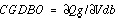 , (for Meyer CGD=-CGDBO)
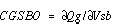 , (for Meyer CGS=-CGSBO)
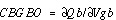 , (for Meyer CGB=-CBGBO)