This section provides details of the requirements for T line or U line simulation.
The ideal transmission line element contains the element name, connecting nodes, characteristic impedance (Z0), and wire delay (TD), unless Z
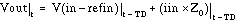
The input and output of the ideal transmission line have the following relationships:
The signal delays for ideal transmission lines are given by:
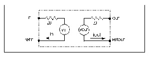
The ideal transmission line only delays the difference between the signal and the reference. Some applications, such as a differential output driving twisted pair cable, require both differential and common mode propagation. Use a U Element, if you need the full signal and reference. You can use approximately two T Elements (as shown in Figure Use of Two T Elements for Full Signal and Reference). In this figure, the two lines are completely uncoupled, so that only the delay and impedance values are correctly modeled.
You cannot implement coupled lines with the T Element, so use U Elements for applications requiring two or three coupled conductors.
Star-Hspice uses a transient timestep that does not exceed half the minimum line delay. Very short transmission lines (relative to the analysis time step) cause long simulation times. You can replace very short lines with a single R, L, or C Element (see Figure Wire Model Selection Chart).
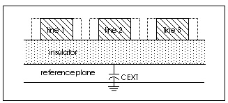
Star-Hspice uses a U Element to model single and coupled lossy transmission lines for various planar, coaxial, and twinlead structures. When a U Element is included in your netlist, Star-Hspice creates an internal network of R, L, C, and G Elements to represent up to five lines and their coupling capacitances and inductances. For more information, see Using Passive Device Models.
You can specify interconnect properties in three ways:
This section initially describes how to use the third method.
The U model provided with Star-Hspice has been optimized for typical geometries used in ICs, MCMs, and PCBs. The model's closed form expressions are optimized via measurements and comparisons with several different electromagnetic field solvers.
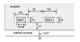
The Star-Hspice U Element geometric model handles one to five uniformly spaced transmission lines, all at the same height. Also, the transmission lines can be on top of a dielectric (microstrip), buried in a sea of dielectric (buried), have reference planes above and below them (stripline), or have a single reference plane and dielectric above and below the line (overlay). Thickness, conductor resistivity, and dielectric conductivity allow for calculating loss as well.
The U Element statement contains the element name, the connecting nodes, the U model reference name, the length of the transmission line, and, optionally, the number of lumps in the element. You can create two kinds of lossy lines: lines with a reference plane inductance (LRR, controlled by the model parameter LLEV) and lines without a reference plane inductance. Wires on integrated circuits and printed circuit boards require reference plane inductance.
The reference ground inductance and the reference plane capacitance to SPICE ground are set by the HGP, CMULT, and optionally, the CEXT parameters.
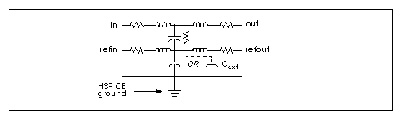
The schematic for a single lump of the U model, with LLEV=0, is shown in Lossy Line with Reference Plane. If LLEV is 1, the schematic includes inductance in the reference path as well as capacitance to HSPICE ground. See the section, Reference Planes and HSPICE Ground for more information about LLEV=1 and reference planes.
The following describes Star-Hspice netlist syntax for the U model. Tables U Element Physical Parameters and U Element Loss Parameters list the model parameters.
.MODEL mname U LEVEL=3 ELEV=val PLEV=val <DLEV=val>
+ <LLEV=val> + <Pname=val> ...
|
Selects the electrical specification format including the geometric model |
|
|
Selects the use of reference plane inductance and capacitance to HSPICE ground. |
|
|
Specifies a physical parameter, such as NL or WD (see U Element Physical Parameters) or a loss parameter, such as RHO or NLAY (see U Element Loss Parameters). |
Dielectric and Reference Plane Configurations shows the three dielectric configurations for the geometric U model. You use the DLEV switch to specify one of these configurations. The geometric U model uses ELEV=1.
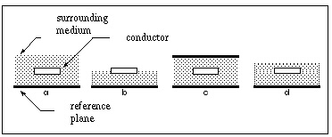
In Dielectric and Reference Plane Configurations a) sea, DLEV=0, b) microstrip, DLEV=1, c) stripline, DLEV=2 and d) overlay, DLEV=3
The parameters for U models are shown in U Element Physical Parameters.
There are two parametric adjustments in the U model: XW, and CORKD. XW adds to the width of each conductor, but does not change the conductor pitch (spacing plus width). XW is useful for examining the effects of conductor etching. CORKD is a multiplier for the dielectric value. Some board materials vary more than others, and CORKD provides an easy way to test tolerance to dielectric variations.
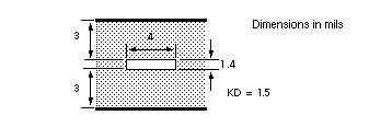
The dimensions for one and two-conductor planar transmission lines are shown in U Element Conductor Dimensions.
Loss parameters for the U model are shown in U Element Loss Parameters.
Losses have a large impact on circuit performance, especially as clock frequencies increase. RHO, RHOB, SIG, and NLAY are parameters associated with losses. Time domain simulators, such as SPICE, cannot directly handle losses that vary with frequency. Both the resistive skin effect loss and the effects of dielectric loss create loss variations with frequency. NLAY is a switch that turns on skin effect calculations in Star-Hspice. The skin effect resistance is proportional to the conductor and backplane resistivities, RHO and RHOB.
The dielectric conductivity is included through SIG. The U model computes the skin effect resistance at a single frequency and uses that resistance as a constant. The dielectric SIG is used to compute a fixed conductance matrix, which is also constant for all frequencies. A good approximation of losses can be obtained by computing these resistances and conductances at the frequency of maximum power dissipation. In AC analysis, resistance increases as the square root of frequency above the skin-effect frequency, and resistance is constant below the skin effect frequency.
The U Element analytic equations compute quickly, but have a limited range of validity. The U Element equations were optimized for typical IC, MCM, and PCB applications. Recommended Ranges lists the recommended minimum and maximum values for U Element parameter variables.
The U Element equations lose their accuracy when you use values outside the recommended ranges. Because the single-line formula is optimized for single lines, you will notice a difference between the parameters of single lines and two coupled lines at a very wide separation. The absolute error for a single line parameter is less than 5% when used within the recommended range. The main line error for coupled lines is less than 15%. Coupling errors can be as high as 30% in cases of very small coupling. Since the largest errors occur at small coupling values, actual waveform errors are kept small.
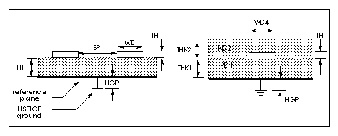
Schematic of a U Element Lump when LLEV=1 shows a single lump of a U model, for a single line with reference plane inductance. When LLEV=1, the reference plane inductance is computed, and capacitance from the reference plane to HSPICE ground is included in the model. The reference plane is the ground plane of the conductors in the U model.
The model reference plane is not necessarily the same as HSPICE ground. For example, a printed circuit board with transmission lines can have a separate reference plane above a chassis. Star-Hspice uses either HGP, the distance between the reference plane and HSPICE ground, or Cext to compute the parameters for the ground-to-reference transmission line.
When HGP is used, the capacitance per meter of the ground-to-reference line is computed based on a planar line of width (NL+2)(WD+SP) and the height of HGP above the SPICE ground. CMULT is used as the dielectric constant of the ground-to-reference transmission line. If Cext is given, then Cext is used as the capacitance per meter for the ground-to-reference line. The inductance of the ground-to-reference line is computed from the capacitance per meter and an assumed propagation at the speed of light.
Most of the power in a transmission line is dissipated at the clock frequency. As a first choice, Star-Hspice estimates the maximum dissipation frequency, or skin effect frequency, from the risetime parameter. The risetime parameter is set with the .OPTION statement (for example, .OPTION RISETIME=0.1ns).
Some designers use 0.35/trise to estimate the skin effect frequency. This estimate is good for the bandwidth occupied by a transient, but not for the clock frequency, at which most of the energy is transferred. In fact, a frequency of 0.35/trise is far too high and results in excessive loss for almost all applications. Star-Hspice computes the skin effect frequency from 1/(15*trise). If you use precomputed model parameters (ELEV = 2), compute the resistance matrix at the skin effect frequency.
When the risetime parameter is not given, Star-Hspice uses other parameters to compute the skin effect frequency. Star-Hspice examines the .TRAN statement for tstep and delmax and examines the source statement for trise. If you set any one of the parameters tstep, delmax, and trise, Star-Hspice uses the maximum of these parameters as the effective risetime.
In AC analysis, the skin effect is evaluated at the frequency of each small-signal analysis. Below the computed skin effect frequency (ELEV=1) or FR1(ELEV=3), the AC resistance is constant. Above the skin effect frequency, the resistance increases as the square root of frequency.
The number of sections (lumps) in a transmission line model also affects the transmission line response. Star-Hspice computes the default number of lumps from the line delay and the signal risetime. There should be enough lumps in the transmission line model to ensure that each lump represents a length of line that is a small fraction of a wavelength at the highest frequency used. It is easy to compute the number of lumps from the line delay and the signal risetime, using an estimate of 0.35/trise as the highest frequency.
For the default number of lumps, Star-Hspice uses the smaller of 20 or 1+(20*TDeff/trise), where TDeff is the line delay. In most transient analysis cases, using more than 20 lumps gives a negligible bandwidth improvement at the cost of increased simulation time. In AC simulations over many decades of frequency with lines over one meter long, more than 20 lumps may be needed for accurate simulation.
Sometimes a transmission line simulation shows ringing in the waveforms, as in Computed Responses for 20 Lumps and 3 Lumps, Gear and Trapezoidal Integration Methods. If the ringing is not verifiable by measurement, it might be due to an incorrect number of lumps in the transmission line models or due to the simulator integration method. Increasing the number of lumps in the model or changing the integration method to Gear reduces the amount of ringing due to simulation errors. The default Star-Hspice integration method is TRAP (trapezoidal), but you can change it to Gear with the statement .OPTION METHOD=GEAR.
See Oscillations Due to Simulation Errors for more information on the number of lumps and ringing.
The next section covers parameters for geometric lines. Coaxial and twinlead transmission lines are discussed in addition to the previously described planar type.
Geometric parameters provide a description of a transmission line in terms of the geometry of its construction and the physical constants of each layer, or other geometric shape involved.
Planar conductors are used to model printed circuit boards, packages, and integrated circuits. The geometric planar transmission line is restricted to:
Common planar conductors include:
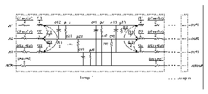
Precomputed parameters allow the specification of up to five signal conductors and a reference conductor. These parameters may be extracted from a field solver, laboratory experiments, or packaging specifications supplied by vendors. The parameters supplied include:
Precomputed Components for Three Conductors and a Reference Plane identifies the precomputed components for a three-conductor line with a reference plane. The Star-Hspice names for the resistance, capacitance, and conductance components for up to five lines are shown in ELEV=2 Model Keywords for Conductor PLEV=1.
All precomputed parameters default to zero except CEXT, which is not used unless it is defined. The units are standard MKS in every case, namely:
Three additional parameters, LLEV (which defaults to 0), CEXT, and GPR are described below.
For the precomputed lossy U model (ELEV=2), the conductor width must be smaller than the reference plane width, which makes the conductor inductance smaller than the reference plane inductance. If the reference plane inductance is greater than the conductor inductance, Star-Hspice reports an error.
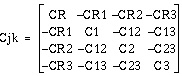
Three different definitions of capacitances and conductances between multiple conductors are currently used. In this manual, relationships are written explicitly only for various capacitance formulations, but they apply equally well to corresponding conductance quantities, which are electrically in parallel with the capacitances. The symbols used in this section, and where one is likely to encounter these usages, are:
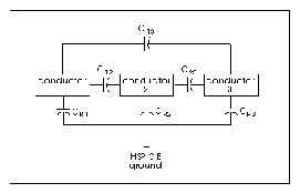
The following example uses a multiple conductor capacitance model, a typical Star-Hspice U model transmission line. The U Element supports up to five signal conductors plus a reference plane, but the three conductor case, Single-Lump Circuit Capacitance, demonstrates the three definitions of capacitance. The branch capacitances are given in Star-Hspice notation.
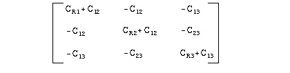
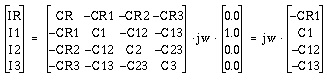
The branch and Maxwell matrices are completely derivable from each other. The "O.C.G." ("other conductors grounded") matrix is derivable from either the Maxwell matrix or the branch matrix. Thus:
Cjk = CX on diagonal
= -CXY off diagonal
The matrices for the example given above provide the following "O.C.G." capacitances:
C1 = CR1 + C12 + C13
C2 = CR2 + C12 + C23
C3 = CR3 + C13 + C23
CR = CR1 + CR2 + CR3 + CPR
Also, the Maxwell matrix is given as:
The branch capacitances also may be obtained from the Maxwell matrices. The off-diagonal terms are the negative of the corresponding Maxwell matrix component. The branch matrix terms for capacitance to circuit ground are the sum of all the terms in the full column of the maxwell matrix, with signs intact:
CP1, ... CP5 are not computed internally with the Star-Hspice geometric (ELEV=1) option, although CPR is. This, and the internally computed inductances, are consistent with an implicit assumption that the signal conductors are completely shielded by the reference plane conductor. This is true, to a high degree of accuracy, for stripline, coaxial cable, and shielded twinlead, and to a fair degree for MICROSTRIP. If accurate values of CP1 and so forth are available from a field solver, they can be used with ELEV=2 type input.
If the currents from each of the other conductors can be measured separately, then all of the terms in the Maxwell matrix may be obtained by laboratory experiment. By setting all voltages except that on the first signal conductor equal to 0, for instance, you can obtain all of the Maxwell matrix terms in column 1.
The advantage of using branch capacitances for input derives from the fact that only one side of the off-diagonal matrix terms are input. This makes the input less tedious and provides fewer opportunities for error.
When measured parameters are specified in the input, the program calculates the resistance, capacitance, and inductance parameters using TEM transmission line theory with the LLEV=0 option. If redundant measured parameters are given, the program recognizes the situation, and discards those which are usually presumed to be less accurate. For twinlead models, PLEV=3, the common mode capacitance is one thousandth of that for differential-mode, which allows a reference plane to be used.
The ELEV=3 model is limited to one conductor and reference plane for PLEV=1.
|
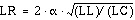
Attenuation factor in length atlen. Use dB scale factor when specifying attenuation in dB. |
|||
|
Frequency at which AT1 is valid. Resistance is constant below FR1, and increases as
|
You can use several combinations of measured parameters to compute the L and C values used internally. The full parameter set is redundant. If you input a redundant parameter set, the program discards those that are presumed to be less accurate. Lossless Parameter Combinations shows how each of seven possible parameter combinations are reduced, if need be, to a unique set and then used to compute C and L.
Three different delays are used in discussing Star-Hspice transmission lines:
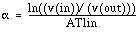
The attenuation per unit length may be specified either as an attenuation factor or as a decibel attenuation. In order to allow for the fact that the data may be available either as input/output or output/input, decibels greater than 0, or factors greater than 1 are assumed to be input/output. The following example shows the four ways that one may specify that an input of 1.0 is attenuated to an output of 0.758.
The attenuation factor is used to compute the exponential loss parameter and linear resistance.
The following examples show the results of simulating a stripline geometry using the U model in a PCB scale application and in an IC scale application.
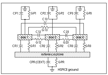
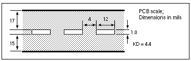
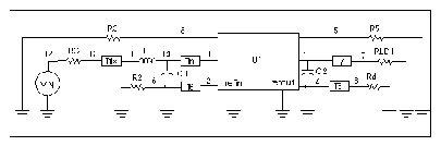
Three Coupled Striplines (PCB Scale) shows three coupled lines in a stripline configuration on an FR4 printed circuit board. A simple circuit using three coupled striplines is shown in Schematic Using the Three Coupled Striplines U Model.
The Star-Hspice input file for the simulation is shown below.
* Stripline circuit
.Tran 50ps 7.5ns
.Options Post NoMod Accurate Probe Method=Gear
VIN 12 0 PWL 0 0v 250ps 0v 350ps 2v
L1 14 11 2.5n
C1 14 0 2p
Tin 14 0 10 0 ZO=50 TD=0.17ns
Tfix 13 0 11 0 ZO=45 TD=500ps
RG 12 13 50
RLD1 7 0 50
C2 1 0 2p
U1 3 10 2 0 5 1 4 0 USTRIP L=0.178
T6 2 0 6 0 ZO=50 TD=0.17ns
T7 1 0 7 0 ZO=50 TD=0.17ns
T8 4 0 8 0 ZO=50 TD=0.17ns
R2 6 0 50
R3 3 0 50
R4 8 0 50
R5 5 0 50
.Model USTRIP U LEVEL=3 PLev=1 Elev=1 Dlev=2 Nl=3 Ht=381u
+ Wd=305u Th=25u Sp=102u Ts=838u Kd=4.7
.Probe v(13) v(7) v(8)
.End
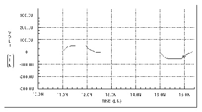
Figures Measured versus Computed Through-Line Response, Measured Versus Computed Backward Crosstalk Response, and Measured Versus Computed Forward Crosstalk Response show the main line and crosstalk responses. The rise time and delay of the waveform are sensitive to the skin effect frequency, since losses reduce the slope of the signal rise. The main line response shows some differences between simulation and measurement. The rise time differences are due to layout parasitics and the fixed resistance model of skin effect. The differences between measured and simulated delays are due to errors in the estimation of dielectric constant and the probe position.
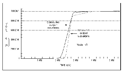
The gradual rise in response between 3 ns and 4 ns is due to skin effect. During this period, the electric field driving the current penetrates farther into the conductor so that the current flow increases slightly and gradually. This affects the measured response as shown for the period between 3 ns and 4 ns.
Measured Versus Computed Backward Crosstalk Response shows the backward crosstalk response. The amplitude and delay of this backward crosstalk are very close to the measured values. The risetime differences are due to approximating the skin effect with a fixed resistor, while the peak level difference is due to errors in the LC matrix solution for the coupled lines.
Measured Versus Computed Forward Crosstalk Response shows the forward crosstalk response. This forward crosstalk shows almost complete signal cancellation in both measurement and simulation. The forward crosstalk levels are about one tenth the backward crosstalk levels. The onset of ringing of the forward crosstalk has reasonable agreement between simulation and measurement. However, the trailing edge of the measured and simulated responses differ. The measured response trails off to zero after about 3 ns, while the simulated response does not trail down to zero until 6 ns. Errors in simulation at this voltage level can easily be due to board layout parasitics that have not been included in the simulation.
Simulation methods can have a significant effect on the predicted waveforms. Computed Responses for 20 Lumps and 3 Lumps, Gear and Trapezoidal Integration Methods shows the main line response at Node 7 of Schematic Using the Three Coupled Striplines U Model as the integration method and the number of lumped elements change. With the recommended number of lumps, 20, the Trapezoidal integration method shows a fast risetime with ringing, while the Gear integration method shows a fast risetime and a well damped response. When the number of lumped elements is changed to 3, both Trapezoidal and Gear methods show a slow risetime with ringing. In this situation, the Gear method with 20 lumps gives the more accurate simulation.
This example shows the U Element analytic equations for a typical integrated circuit transmission line application. Three 200µm-long aluminum wires in a silicon dioxide dielectric are simulated to examine the through-line and coupled line response.
The Star-Hspice U model uses the transmission line geometric parameters to generate a multisection lumped-parameter transmission line model. Star-Hspice uses a single U Element statement to create an internal network of three 20-lump circuits.
Three Coupled Lines with One Reference Plane in a Sea of Dielectric (IC Scale) shows the IC-scale coupled line geometry.
Schematic for Three Coupled Lines with One Reference Plane shows one lump of the lumped-parameter schematic for the three-conductor stripline configuration of Three Coupled Lines with One Reference Plane in a Sea of Dielectric (IC Scale). This is the internal circuitry Star-Hspice creates to represent one U Element instantiation. The internal elements are described in Star-Hspice Output.
Schematic Using the Three Coupled Lines U Model shows a schematic using the U Element of Schematic for Three Coupled Lines with One Reference Plane. In this simple circuit, a pulse drives a three-conductor transmission line source terminated by 50 resistors and loaded by 1pF capacitors.
The Star-Hspice input file for the U Element solution is shown below.
.Tran 0.1ns 20ns
.Options Post Accurate NoMod Brief Probe
Vss Vss 0 0v
Rss Vss 0 1x
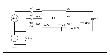
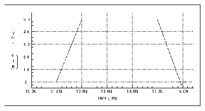
vIn1 In1 Vss Pwl 0ns 0v 11ns 0v 12ns 5v 15ns 5v 16ns 0v
rIn1 In1 In10 50
rIn2 Vss In20 50
rIN3 Vss In30 50
u1 In10 In20 In30 Vss Out1 Out2 Out3 Vss IcWire L=200um
cIn1 Out1 Vss 1pF
cIn2 Out2 Vss 1pF
cIn3 Out3 Vss 1pF
.Probe v(Out1) v(Out2) v(Out3)
.Model IcWire U LEVEL=3 Dlev=0 Nl=3 Nlay=2 Plev=1 Elev=1
+ Llev=0 Ht=2u Wd=5u Sp=15u Th=1u Rho=2.8e-8 Kd=3.9
.End
The Star-Hspice U Element uses the conductor geometry to create length-independent RLC matrices for a set of transmission lines. You can then input any length, and Star-Hspice computes the number of circuit lumps that are required.
Computed Through-Line Response, Computed Nearest Coupled-Line Response, and Computed Furthest Coupled-Line Response show the through and coupled responses computed by Star-Hspice using the U Element equations.
Computed Nearest Coupled-Line Response shows the nearest coupled line response. This response only occurs during signal transitions.
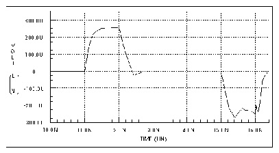
Computed Furthest Coupled-Line Response shows the third coupled line response. The predicted response is about 1/100000 of the main line response.
By default, Star-Hspice prints the model values, including the LCRG matrices, for the U Element. All of the LCRG parameters printed by Star-Hspice are identified in the following section.
The listing below is part of the Star-Hspice output from a simulation using the HSPICE input deck for the IcWire U model. Descriptions of the parameters specific to U Elements follows the listing. (Parameters not listed in this section are described in Tables U Element Physical Parameters and U Element Loss Parameters.)
*** model name: 0:icwire ****
names values units names values units names values units
----- ------ ----- ----- ------ ----- ----- ------ -----
--- u-model control parameters ---
maxl= 20.00 #lumps wlump= 20.00 elev= 1.00
plev= 1.00 llev= 0. nlay= 2.00 #layrs
nl= 3.00 #lines nb= 1.00 #refpl
--- begin type specific parameters ---
dlev= 0. # kd= 3.90 corkd= 1.00
sig= 0. mho/m rho= 28.00n ohm*m rhob= 28.00n ohm*m
xw= 0. meter wd= 5.00u meter ht= 2.00u meter
th= 1.00u meter thb= 1.42u meter skin= 10.31u meter
skinb= 10.31u meter wd2 5.00u meter ht2 2.00u meter
th2 1.00u meter sp1 15.00u meter wd3 5.00u meter
ht3 2.00u meter th3 1.00u meter sp2 15.00u meter
cr1= 170.28p f/m gr1= 0. mho/m l11= 246.48n h/m
cr2= 168.25p f/m gr2= 0. mho/m c12= 5.02p f/m
g12= 0. mho/m l12= 6.97n h/m l22= 243.44n h/m
cr3= 170.28p f/m gr3= 0. mho/m c13= 649.53f f/m
g13= 0. mho/m l13= 1.11n h/m c23= 5.02p f/m
g23= 0. mho/m l23= 6.97n h/m l33= 246.48n h/m
--- two layer (skin and core) parameters ---
rrs= 1.12k ohm/m rrc= 0. ohm/m r1s= 5.60k ohm/m
r1c= 0. ohm/m r2s= 5.60k ohm/m r2c= 0. ohm/m
r3s= 5.60k ohm/m r3c= 0. ohm/m
The total conductor resistance is indicated by rjj when NLAY = 1, or by ris + ric when NLAY = 2.
As shown in the next section, some difference between HSPICE and field solver results is to be expected. Within the range of validity shown in Recommended Ranges for the Star-Hspice model, Star-Hspice comes very close to field solver accuracy. In fact, discrepancies between results from different field solvers can be as large as their discrepancies with Star-Hspice. The next section compares some Star-Hspice physical models to models derived using field solvers.
Star-Hspice places capacitance and inductance values for U Elements in matrix form, for example:

Capacitance and Inductance Matrices for the Three-Line, IC-Scale Interconnect System shows the capacitance and inductance matrices for the three-line, buried microstrip IC-scale example shown in Three Coupled Lines with One Reference Plane in a Sea of Dielectric (IC Scale).
The capacitance matrices in Capacitance and Inductance Matrices for the Three-Line, IC-Scale Interconnect System are based on the admittance matrix of the capacitances between the conductors. The negative values in the capacitance matrix are due to the sign convention for admittance matrices. The inductance matrices are based on the impedance matrices of the self and mutual inductance of the conductors. Each matrix value is per meter of conductor length. The actual lumped values used by Star-Hspice would use a conductor length equal to the total line length divided by the number of lumps.
The above capacitance matrix can be related directly to the Star-Hspice output of Example 2. Star-Hspice uses the branch capacitance matrix for internal calculations. For the three-conductors in this example, Conductor Capacitances for Example 2 shows the equivalent capacitances, in terms of Star-Hspice parameters.
The capacitances of Conductor Capacitances for Example 2 are those shown in Schematic for Three Coupled Lines with One Reference Plane. The HSPICE nodal capacitance matrix of Capacitance and Inductance Matrices for the Three-Line, IC-Scale Interconnect System is shown below, using the capacitance terms that are listed in the HSPICE output.
The off-diagonal terms are the negative of the coupling capacitances (to conform to the sign convention). The diagonal terms require some computation, for example,
Note that the matrix values on the diagonal in Capacitance and Inductance Matrices for the Three-Line, IC-Scale Interconnect System are large: they indicate self-capacitance and inductance. The diagonal values show close agreement among the various solution methods. As the coupling values become small compared to the diagonal values, the various solution methods give very different results. Third-line coupling capacitances of 0.65 pF/m, 1.2 pF/m, and 0.88 pF/m are shown in Capacitance and Inductance Matrices for the Three-Line, IC-Scale Interconnect System. Although the differences between these coupling capacitances seem large, they represent a negligible difference in waveforms because they account for only a very small amount of voltage coupling. Capacitance and Inductance Matrices for the Three-Line, IC-Scale Interconnect System represents very small coupling because the line spacing is large (about seven substrate heights).
Capacitance and Inductance for the Single Line MCM-Scale Stripline shows the parameters for the stripline shown in Stripline Geometry Used in MCM Technology.
This example shows a five-line interconnect system in a PCB technology. Capacitance and Inductance for the Five-Line PCB-Scale Interconnect System shows the matrix parameters for the line configuration of Five Coupled Lines on a PCB.
This section gives examples of use, and then explains some of the aspects of ringing (impulse-initiated oscillation) in real and simulated transmission line circuits.
uc in1 3 out1 4 wire2 l=1
.model wire2 u LEVEL=3 nlay=2 plev=2 elev=1 Llev=1
+ ra=1m rb=7.22m hgp=20m rho=1.7e-8 kd=2.5
u1 In1 In2 In3 Vss Out1 Out2 Out3 Vss Wire3 L=0.01
.model Wire3 U LEVEL=3 NL=3 Elev=2 Llev=0
+ rrr=1.12k r11=5.6k r22=5.6k r33=5.6k c13=0.879pF
+ cr1=176.4pF cr2=172.6pF cr3=176.4pF c12=4.7pF c23=4.7pF
+ L11=237nH L22=237nH L33=237nH L12=5.52nH L23=5.52nH
+ L13=1.34nH
u10 1 0 2 0 rg58 l=12
.model rg58 u LEVEL=3 plev=2 elev=3
+ zk=50 capl=30.8p clen=1ft vrel=0.66
+ fr1=100meg at1=5.3db atlen=100ft
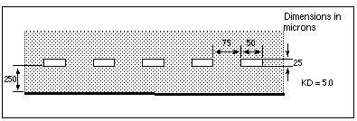
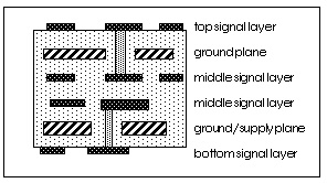
Six-Layer Printed Circuit Board illustrates a small cross section of a six-layer printed circuit board. The top and bottom signal layers require a microstrip U model (DLEV=1), while the middle signal layers use a stripline U model (DLEV=2). Important aspects of such a circuit board are the following:
.MODEL TOP U LEVEL=3 ELEV=1 PLEV=1 TH=1.3mil HT=10mil KD=4.5 DLEV=1
+ WD=8mil XW=-2mil
.MODEL MID U LEVEL=3 ELEV=1 PLEV=1 TH=1.3mil HT=10mil KD=4.5 DLEV=2
+ WD=8mil XW=-2mil TS=32mil
The following examples are for standard coax. These are obtained from commonly available tables
.model rg9/u u LEVEL=3 plev=2 elev=3
+ Zk=51 vrel=.66
+ fr1=100meg at1=2.1db atlen=100ft
*
.model rg9b/u u LEVEL=3 plev=2 elev=3
+ Zk=50 vrel=.66
+ fr1=100meg at1=2.1db atlen=100ft
*
.model rg11/u u LEVEL=3 plev=2 elev=3
+ Zk=75 vrel=.78
+ fr1=100meg at1=1.5db atlen=100ft
*
.model rg11a/u u LEVEL=3 plev=2 elev=3
+ Zk=75 vrel=.66
+ fr1=100meg at1=1.9db atlen=100ft
*
.model rg54a/u u LEVEL=3 plev=2 elev=3
+ Zk=58 vrel=.66
+ fr1=100meg at1=3.1db atlen=100ft
*
.model rg15/u u LEVEL=3 plev=2 elev=3
+ Zk=53.5 vrel=.66
+ fr1=100meg at1=4.1db atlen=100ft
*
.model rg53/u u LEVEL=3 plev=2 elev=3
+ Zk=53.5 vrel=.66
+ fr1=100meg at1=4.1db atlen=100ft
*
.model rg58a/u u LEVEL=3 plev=2 elev=3
+ Zk=50 vrel=.66
+ fr1=100meg at1=5.3db atlen=100ft
*
.model rg58c/u u LEVEL=3 plev=2 elev=3
+ Zk=50 vrel=.66
+ fr1=100meg at1=5.3db atlen=100ft
*
.model rg59b/u u LEVEL=3 plev=2 elev=3
+ Zk=75 vrel=.66
+ fr1=100meg at1=3.75db atlen=100ft
*
.model rg62/u u LEVEL=3 plev=2 elev=3
+ Zk=93 vrel=.84
+ fr1=100meg at1=3.1db atlen=100ft
*
.model rg62b/u u LEVEL=3 plev=2 elev=3
.model tw/sh u LEVEL=3 plev=3 elev=3
* Shielded TV type twinlead
+ Zk=300 vrel=.698
+ fr1=57meg at1=1.7db atlen=100ft
*
.model tw/un u LEVEL=3 plev=3 elev=3
* Unshielded TV type twinlead
+ Zk=300 vrel=.733
+ fr1=100meg at1=1.4db atlen=100ft
Two Coupled Microstrips Geometrically Defined as LSI Metallization shows two metal lines formed of the first aluminum layer of a modern CMOS process. The microstrip model assumes that the metal strips sit on top of a dielectric layer that covers the reference plane.
* file strip2.sp Two microstrips coupled together
*.... The tests following use geometric/physical model
.option acct post list
.print tran V(no1) V(no2) V(noref)
.tran 1ps 300ps
.PARAM Rx=54
* excitation voltage + prefilter
V1 np1 0 PWL 0.0s 0v 50ps 0v 60ps 1v
xrI1 NP1 NI1 rcfilt rflt=rx tdflt=1ps
Ue1 NI1 NI2 0 NO1 NO2 NORef u1 L=5.0m
RI2 NI2 0 Rx
RO1 NO1 NORef Rx
RO2 NO2 NORef Rx
rref noref 0 1
* ...MODEL DEFINITION -- metal layer1 (sea of dielectric)
.MODEL u1 U LEVEL=3 plev=1 elev=1 nl=2
+ KD=3.5 xw=0.1u rho=17e-9 rhob=20e-9
+ wd=1.5u ht=1.0u th=0.6u sp=1.5u
+ llev=1 dlev=0 maxl=50
*
.END
Ringing oscillations at sharp signal edges may be produced by:
The primary reason for using a circuit simulator to measure high speed transmission line effects is to calculate how much transient noise the system contains and to determine how to reduce it to acceptable values.
The system noise results from the signal reflections in the circuit. It may be masked by noises from the simulator. Simulator noise must be eliminated in order to obtain reliable system noise estimates. The following sections describes ways to solve problems with simulator noise.
The default method of integrating inductors and capacitors is trapezoidal integration. While this method gives excellent results for most simulations, it can lead to what is called trapezoidal ringing. This is numerical oscillations that look like circuit oscillations, but are actually timestep control failures. In particular, trapezoidal ringing can be caused by any discontinuous derivatives in the nonlinear capacitance models, or from the exponential charge expressions for diodes, BJTs, and JFETs.
Set the .OPTION METHOD=GEAR to change the integration method from trapezoidal to Gear. The gear method does not ring and, although it typically gives a slightly less accurate result, is still acceptable for transient noise analysis.
It is important to use the right number of lumps in a lossy transmission line element. Too few lumps results in false ringing or inaccurate signal transmission, while too many lumps leads to an inordinately long simulation run. Sometimes, as in verification tests, it is necessary to be able to specify the number of lumps in a transmission line element directly. The number of lumps in an Star-Hspice lossy transmission line element may be directly specified, defaulted to an accuracy and limit based computation, or computed with altered accuracy and limit and risetime parameters.
In the default computation, LUMPS=1 until a threshold of total delay versus risetime is reached:
|
TDeff = total end-to-end delay in the transmission line element |
|
|
RISETIME = the duration of the shortest signal ramp, as given in the statement |
At the threshold, two lumps are used. Above the threshold, the number of lumps is determined by:
number of lumps = minimum of 20 or [1+(TDeff/RISETIME)*20]
The upper limit of 20 is applied to enhance simulation speed.
If the standard accuracy-based computation does not provide enough lumps, or if it computes too many lumps for simulation efficiency, you can use one of several methods to change the number of lumps on one or more elements:
1. Specify LUMPS=value in the element statement.
2. Specify MAXL=value and WLUMP=value in the .MODEL statement.
3. Specify a different RISETIME=value in the .OPTION statement.
Direct specification overrides the model and limit based computation, applying only to the element specified in the element statement, as in the example below:
U35 n1 gnd n2 oref model lumps=31 L=5m
where 31 lumps are specified for an element of length 5 mm.
You can alter the default computation for all the elements that refer to a particular model by specifying the model parameters "MAXL" and "WLUMP" (which would otherwise default to 20). In the nondefault case the number of lumps, the threshold, and the upper limit all would be changed:
lumps = min{MAXL, [1+(TDeff/RISETIME)*WLUMP]}
Threshold: TDeff = RISETIME/WLUMP
Upper lim: MAXL
You can change the threshold and number of lumps computed for all elements of all models, reduce or increase the analysis parameter "RISETIME". Note that care is required if RISETIME is decreased, because the number of lumps may be limited by MAXL in some cases where it was not previously limited.
Artificial sources such as pulse and piecewise linear sources often are used to simulate the action of real output buffer drivers. Since real buffers have a finite cutoff frequency, a multistage filter can be used to give the ideal voltage source reasonable impedance and bandwidth.
You can place a multistage RC filter, shown below, between the artificial source and any U Element to reduce the unrealistic source bandwidth and, consequently, the unrealistic ringing. In order to provide as much realism as possible, the interposed RC filter and the PWL (piecewise linear) source must be designed together to meet the following criteria:
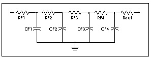
.MACRO RCFNEW in out gnd_ref RFLT=50 TDFLT=100n
*
.PROT
* Begin RCFILT.inc (RC filter) to smooth and match pulse
* sources to transmission lines. User specifies impedance
* (RFLT) and smoothing interval (TDFLT). TDFLT is usually
* specified at about .1*risetime of pulse source.
*
* cuttoff freq, total time delay; and frequency dependent
* impedance and signal voltage at "out" node:
*
* smoothing period = TDFLT.....(equivalent boxcar filter)
* delay= TDFLT
* fc=2/(pi*TDFLT)..............(cuttoff frequency)
* Zo~ RFLT*(.9 + .1/sqrt( 1 + (f/fc)^2 )
* V(out)/V(in)= [1 / sqrt( 1 + (f/fc)^2 )]^4
*
.PARAM TD1S='TDFLT/4.0'
RF1 in n1 `.00009*RFLT'
RF2 n1 n2 `.0009*RFLT'
RF3 n2 n3 `.009*RFLT'
RF4 n3 n4 `.09*RFLT'
Rout n4 out `.90*RFLT'
*
.PARAM CTD='TD1S/(.9*RFLT)'
CF1 n1 0 `10000*CTD'
CF2 n2 0 `1000*CTD'
CF3 n3 0 `100*CTD'
CF4 n4 0 `10*CTD'
*
.UNPROT
.EOM
From the comments embedded in the macro, the output impedance varies from RFLT in the DC limit to 3% less at FC and 10% less in the high frequency limit.
Therefore, setting RFLT to the desired driver impedance gives a reasonably good model for the corrected driver impedance. TDFLT is generally set to 40% of the voltage source risetime.
* excitation voltage + prefilter
V1 np1 0 PWL 0.0s 0v 50ps 0v 60ps 1v
xrI1 NP1 NI1 RCFNEW rflt=rx tdflt=4ps
Multistage RC Filter Input and Output shows the input and output voltages for the filter.
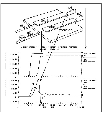
The effect of impedance mismatch is demonstrated in the following example. This circuit has a 75 ohm driver, driving 3 inches of 8 mil wide PCB (middle layer), then driving 3 inches of 16 mil wide PCB.
The operational characteristics of such a circuit are shown in Figures Mathematical Transmission Line Structure, Waveforms in Mismatched Transmission Line Structure, and Impedance from TDR at Input. The first steady value of impedance is 75 ohms, which is the impedance of the first transmission line section. The input impedance falls to 56 ohms after about 2.5ns, when the negative reflection from the nx1 node reaches nil. This TDR displays one idiosyncrasy of the U Element. The high initial value of Zin(TDR) is due to the fact that the input element of the U Element is inductive. The initial TDR spike can be reduced in amplitude and duration by simply using a U Element with a larger number of lumped elements.
* file strip1.sp
* Two series microstrips (8mil wide & 16mil) drive 3 inches of 8mil
* middle layer PCB, series connected to 3 inches of 16mil wide
* middle layer PCB, 500ns risetime driver. The tests following use
* geometric/physical model
.option acct post list
.tran 20ps 4ns
.probe tdr=par(`v(ni1)/i(ue1)')
.PARAM R8mil=75 r16mil=56
* excitation voltage + prefilter
V1 np1 0 PWL 0.0s 0v 500ps 0v 1n 1v
xrI1 NP1 NI1 rcfilt rflt=r8mil tdflt=50ps
Ue1 NI1 0 NX1 0 u1 L=3000mil
Ue2 NX1 0 NO2 0 u2 L=3000mil
RO2 NO2 0 r16mil
* ...MODEL DEFINITION -- 8mil middle metal layer of a copper PCB
.MODEL u1 U LEVEL=3 plev=1 elev=1 nl=1
+ th=1.3mil ht=10mil ts=32mil kd=4.5 dlev=0
+ wd=8mil xw=-2mil
* ...MODEL DEFINITION -- 16mil middle metal layer of a copper PCB
.MODEL u2 U LEVEL=3 plev=1 elev=1 nl=1
+ th=1.3mil ht=10mil ts=32mil kd=4.5 dlev=0
+ wd=16mil xw=-2mil
.ENDStar-Hspice Manual - Release 2001.2 - June 2001


 (frequency) above FR1.