This circuit uses the behavioral elements to implement inverters, 2, 3, and 4 input NAND gates.
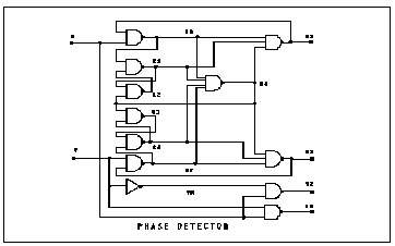
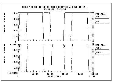
pdb.sp phase detector using behavioral nand gates.
.option post=2
.tran .25n 50ns
*.graph tran v(r) v(v) v(u1)
*.graph tran v(r) v(v) v(u2) $ v(d2)
.probe tran v(r) v(v) v(u1)
.probe tran v(r) v(v) v(u2) $ v(d2)
xnr r u1 nr nand2 capout=.1p
xq1 nr q2 q1 nand2 capout=.1p
xq2 q1 n4 q2 nand2
xq3 q4 n4 q3 nand2
xq4 q3 nv q4 nand2
xnv v d1 nv nand2
xu1 nr q1 n4 u1 nand3
xd1 nv q4 n4 d1 nand3
xvn v vn inv
xu2 vn r u2 nand2
xd2 r v d2 nand2
xn4 nr q1 q4 nv n4 nand4
*
* waveform vv lags waveform vr
vr r 0 pulse(0,5,0n,1n,1n,15n,30n)
vv v 0 pulse(0,5,5n,1n,1n,15n,30n)
*
* waveform vr lags waveform vv
*vr r 0 pulse(0,5,5n,1n,1n,15n,30n)
*vv v 0 pulse(0,5,0n,1n,1n,15n,30n)
.SUBCKT inv in out capout=.1p
cout out 0 capout
rout out 0 1.0k
gn 0 out nand(1) in 0 scale=1
+ 0. 4.90ma
+ 0.25 4.88ma
+ 0.5 4.85ma
+ 1.0 4.75ma
+ 1.5 4.42ma
+ 3.5 1.00ma
+ 4.000 0.50ma
+ 4.5 0.2ma
+ 5.0 0.1ma
.ENDS inv
*
.SUBCKT nand2 in1 in2 out capout=.15p
cout out 0 capout
rout out 0 1.0k
gn 0 out nand(2) in1 0 in2 0 scale=1
+ 0. 4.90ma
+ 0.25 4.88ma
+ 0.5 4.85ma
+ 1.0 4.75ma
+ 1.5 4.42ma
+ 3.5 1.00ma
+ 4.000 0.50ma
+ 4.5 0.2ma
+ 5.0 0.1ma
.ENDS nand2
*
.SUBCKT nand3 in1 in2 in3 out capout=.2p
cout out 0 capout
rout out 0 1.0k
gn 0 out nand(3) in1 0 in2 0 in3 0 scale=1
+ 0. 4.90ma
+ 0.25 4.88ma
+ 0.5 4.85ma
+ 1.0 4.75ma
+ 1.5 4.42ma
+ 3.5 1.00ma
+ 4.000 0.50ma
+ 4.5 0.2ma
+ 5.0 0.1ma
.ENDS nand3
*
.SUBCKT nand4 in1 in2 in3 in4 out capout=.5p
cout out 0 capout
rout out 0 1.0k
gn 0 out nand(4) in1 0 in2 0 in3 0 in4 0 scale=1
+ 0. 4.90ma
+ 0.25 4.88ma
+ 0.5 4.85ma
+ 1.0 4.75ma
+ 1.5 4.42ma
+ 3.5 1.00ma
+ 4.000 0.50ma
+ 4.5 0.2ma
+ 5.0 0.1ma
.ENDS nand4
.end
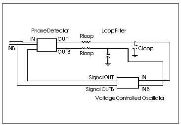
A Phase Locked Loop (PLL) circuit synchronizes to an input waveform within a selected frequency range, returning an output voltage proportional to variations in the input frequency. It has three basic components: a voltage controlled oscillator (VCO), which returns an output waveform proportional to its input voltage, a phase detector which compares the VCO output to the input waveform and returns an output voltage depending on their phase difference, and a loop filter, which filters the phase detector voltage, returning an output voltage which forms the VCO input and the external voltage output of the PLL.
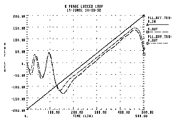
The following example shows a Star-Hspice simulation of a full bipolar implementation of a PLL; its transfer function shows a linear region of voltage vs. (periodic) time which is defined as the "lock" range. The phase detector is modeled behaviorally, effectively implementing a logical XNOR function. This model was then substituted into the full PLL circuit and resimulated. The behavioral model for the VCO was then substituted into the PLL circuit, and this behavioral PLL was then simulated. The results of the transient simulations (Behavioral (PLL_BVP Curve) vs. Bipolar (PLL_BJT Curve) Circuit Simulation) show minimal difference between implementations, but from the standpoint of run time statistics, the behavioral model shows a factor of five reduction in simulation time versus that of the full circuit.
Include the behavioral model if you use this PLL in a larger system simulation (for example, an AM tracking system) because it substantially reduces run time while still representing the subcircuit accurately.
This is an example of a phase locked loop:
$ phase locked loop
.option post probe acct
.option relv=1e-5
$
$ wideband FM example, Grebene gives:
$ f0=1meg kf=250kHz/V
$ kd=0.1 V/rad
$ R=10K C=1000p
$ f_lock = kf*kd*pi/2 = 39kHz, v_lock = kd*pi/2 = 0.157
$ f_capture/f_lock ~= 1/sqrt(2*pi*R*C*f_lock)
$ = 0.63, v_capture ~= 0.100
*.ic v(out)=0 v(fin)=0
.tran .2u 500u
.option delmax=0.01u interp
.probe v_in=v(inc,0) v_out=v(out,outb)
.probe v(in) v(osc) v(mout) v(out)
vin inc 0 pwl 0u,-0.2 500u,0.2
*vin inc 0 0
xin inc 0 in inb vco f0=1meg kf=125k phi=0 out_off=0 out_amp=0.3
$ vco
xvco e eb osc oscb vco f0=1meg kf=125k phi=0 out_off=-1 out_amp=0.3
$ phase detector
xpd in inb osc oscb mout moutb pd kd=0.1 out_off=-2.5
$ filter
rf mout e 10k
cf e 0 1000p
rfb moutb eb 10k
cfb eb 0 1000p
$ final output
rout out e 100k
cout out 0 100p
routb outb eb 100k
coutb outb 0 100p
.macro vco in inb out outb f0=100k kf=50k phi=0.0 out_off=0.0 out_amp=1.0
gs 0 s poly(2) c 0 in inb 0 `6.2832e-9*f0' 0 0 `6.2832e-9*kf'
gc c 0 poly(2) s 0 in inb 0 `6.2832e-9*f0' 0 0 `6.2832e-9*kf'
cs s 0 1e-9
cc c 0 1e-12
e1 s_clip 0 pwl(1) s 0 -0.1,-0.1 0.1,0.1
eout 0 s_clip 0 out_off vol=`10*out_amp'
eboutb 0 s_clip 0 out_off vol=`-10*out_amp'
.ic v(s)='sin(phi)' v(c)='cos(phi)'
.eom
.macro pd in inb in2 in2b out outb kd=0.1 out_off=0
e1 clip1 0 pwl(1) in inb -0.1,-0.1 0.1,0.1
e2 clip2 0 pwl(1) in2 in2b -0.1,-0.1 0.1,0.1
e3 n1 0 poly(2) clip1 0 clip2 0 0 0 0 0 `78.6*kd'
e4 outb 0 n1 0 out_off 1
e5 out 0 n1 0 out_off -1
.eom
.end
This is an example of a BJT LEVEL Voltage Controlled Oscillator (VCO):
$ phase locked loop
.option post probe acct
.option relv=1e-5
$
$ wideband FM example, Grebene gives:
$ f0=1meg kf=250kHz/V
$ kd=0.1 V/rad
$ R=10K C=1000p
$ f_lock = kf*kd*pi/2 = 39kHz, v_lock = kd*pi/2 = 0.157
$ f_capture/f_lock ~= 1/sqrt(2*pi*R*C*f_lock)
$ = 0.63, v_capture ~= 0.100
*.ic v(out)=0 v(fin)=0
.tran .2u 500u
.option delmax=0.01u interp
.probe v_in=v(inc,0) v_out=v(out,outb)
.probe v(in) v(osc) v(mout) v(out) v(e)
vcc vcc 0 6
vee vee 0 -6
$ input
vin inc 0 pwl 0u,-0.2 500u,0.2
xin inc 0 in inb vco f0=1meg kf=125k phi=0 out_off=0 out_amp=0.3
$ vco
xvco1 e eb osc oscb 0 vee vco1
.ic v(osc)=-1.4 v(oscb)=-0.7
$ phase detector
xpd1 in inb osc oscb mout moutb vcc vee pd1
rf mout e 10k
cf e 0 1000p
rfb moutb eb 10k
cfb eb 0 1000p
rout out e 100k
cout out 0 100p
routb outb eb 100k
coutb outb 0 100p
.macro vco in inb out outb f0=100k kf=50k phi=0.0 out_off=0.0 out_amp=1.0
gs 0 s poly(2) c 0 in inb 0 `6.2832e-9*f0' 0 0 `6.2832e-9*kf'
gc c 0 poly(2) s 0 in inb 0 `6.2832e-9*f0' 0 0 `6.2832e-9*kf'
cs s 0 1e-9
cc c 0 1e-9
e1 s_clip 0 pwl(1) s 0 -0.1,-0.1 0.1,0.1
e out 0 s_clip 0 out_off `10*out_amp'
eb outb 0 s_clip 0 out_off `-10*out_amp'
.ic v(s)='sin(phi)' v(c)='cos(phi)'
.eom
.macro pd in inb in2 in2b out outb kd=0.1 out_off=0
e1 clip1 0 pwl(1) in inb -0.1,-0.1 0.1,0.1
e2 clip2 0 pwl(1) in2 in2b -0.1,-0.1 0.1,0.1
e3 n1 0 poly(2) clip1 0 clip2 0 0 0 0 0 `78.6*kd'
e4 outb 0 n1 0 out_off 1
e5 out 0 n1 0 out_off -1
.eom
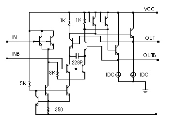
.macro vco1 in inb e7 e8 vcc vee vco_cap=228.5p
qout vcc vcc b7 npn1
qoutb vcc vcc b8 npn1
rb vcc c0 5k $ 1ma
q0 c0 b0 vee npn1
q7 vcc b7 e7 npn1
r4 vcc b7 1k
i7 e7 0 1m
q8 vcc b8 e8 npn1
r5 vcc b8 1k
i8 e8 0 1m
q9 b7 e8 e9 npn1
q10 b8 e7 e10 npn1
c0 e9 e10 vco_cap
q11 e9 in 2 npn1 $ ic=i0
q12 e10 in 2 npn1 $ ic=i0
q15 2 c0 b0 npn1 $ ic=2*i0
q16 3 c0 b0 npn1 $ ic=2*i0
rx 2 3 8k
q13 vcc inb 3 npn1
q14 vcc inb 3 npn1
rt b0 vee 350 $ i=4*i0=2m
.eom
.model npn1 npn
+ eg=1.1 af=1 xcjc=0.95 subs=1
+ cjs=0 tf=5p
+ tr=500p cje=0.2p cjc=0.2p fc=0.8
+ vje=0.8 vjc=0.8 mje=0.33 mjc=0.33
+ rb=0 rbm=0 irb=10u
+ is=5e-15 ise=1.5e-14 isc=0
+ vaf=150 bf=100 ikf=20m
+ var=30 br=5 ikr=15m
+ rc=0 re=0
+ nf=1 ne=1.5 nc=1.2
+ tbf1=8e-03
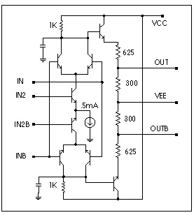
.macro pd1 in inb in2 in2b out outb vcc vee
rl vcc n1 1k
rlb vcc n1b 1k
q3 n1 in c1 npn1
q4 n1b inb c1 npn1
q5 n1 inb c2 npn1
q6 n1b in c2 npn1
q1 c1 in2 e npn1
q2 c2 in2b e npn1
ie e 0 0.5m
c1 n1 0 1p
c1b n1b 0 1p
q7 vcc n1 e7 npn1
q8 vcc n1b e8 npn1
r1 e7 out 625
r2 out vee 300
r1b e8 outb 625
r2b outb vee 300
.eom
.end