This section describes the benefits of using Star-Hspice's op-amps, comparators, and oscillators when performing simulation.
Star-Hspice uses the model generator for the automatic design and simulation of both board level and IC op-amp designs. You can take the existing electrical specifications for a standard industrial operational amplifier, enter the specifications in the op-amp model statement, and Star-Hspice automatically generates the internal components of the op-amp to meet the specifications. You can then call the design from a library for a board level simulation.
The Star-Hspice op-amp model is a subcircuit that is about 20 times faster to simulate than an actual transistor level op-amp. You can adjust the AC gain and phase to within 20 percent of the actual measured values and set the transient slew rates accurately. This model does not contain high order frequency response poles and zeros and may significantly differ from actual amplifiers in predicting high frequency instabilities. Normal amplifier characteristics, including input offsets, small signal gain, and transient effects are represented in this model.
The op-amp subcircuit generator consists of two parts, a model and one or more elements. Each element is in the form of a subcircuit call. The model generates an output file of the op-amp equivalent circuit for collection in libraries. The file name is the name of the model (mname) with an .inc extension.
Once the output file is generated, other Star-Hspice input files may reference this subcircuit using a .SUBCKT call to the model name. The .SUBCKT call automatically searches the present directory for the file, then the directories specified in any .OPTION SEARCH ='directory_path_name', and finally the directory where the DDL (Discrete Device Library) is located.
The amplifier element references the amplifier model.
If DC convergence problems are encountered with op-amp models created by the model generator, use the .IC or .NODESET statement to set the input nodes to the voltage halfway between the VCC and VEE. This balances the input nodes and stabilizes the model.
xa1 in- in+ out vcc vee modelname AV=val
xa1 in- in+ out comp1 comp2 vcc vee modelname AV=val
modelname
.MODEL mname AMP parameter=value ...
mname model name. Elements reference the model by this name.
AMP identifies an amplifier model
parameter any model parameter described below
value value assigned to a parameter
X0 IN- IN+ OUT0 VCC VEE ALM124
.MODEL ALM124 AMP
+ C2= 30.00P SRPOS= .5MEG SRNEG= .5MEG
+ IB= 45N IBOS= 3N VOS= 4M
+ FREQ= 1MEG DELPHS= 25 CMRR= 85
+ ROUT= 50 AV= 100K ISC= 40M
+ VOPOS= 14.5 VONEG= -14.5 PWR= 142M
+ VCC= 16 VEE= -16 TEMP= 25.00
+ PSRR= 100 DIS= 8.00E-16 JIS= 8.00E-16
The model parameters for op-amps are shown below. The defaults for these parameters depend on the DEF parameter setting. Defaults for each of the three DEF settings are shown in the following table.
This example uses the .OPTION AUTOSTOP option to shorten simulation time. Once Star-Hspice makes the measurements specified by the .MEASURE statement, the associated transient analysis and AC analysis stops whether or not the full sweep range for each has been covered.
AC=10000G parameter in the Rfeed element statement installs a 10000 G feedback resistor for the AC analysis in place of the 10 k
 feedback resistor - used in the DC operating point and transient analysis - which is open-circuited for the AC measurements.
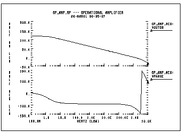
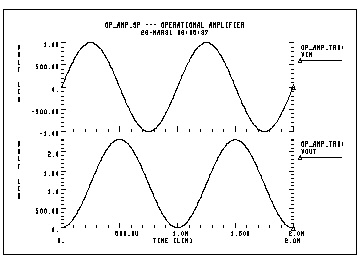
The simulation results give the DC operating point analysis for an input voltage of 0 v and power supply voltages of ±15 v. The DC offset voltage is 3.3021 mv, which is less than that specified for the original vos specification in the op-amp .MODEL statement. The unity gain frequency is given as 907.885 kHz, which is within 10% of the 1 MHz specified in the .MODEL statement with the parameter FREQ. The required time rate for a 1 volt change in the output (from the .MEASURE statement) is 2.3 µs (from the SRPOS simulation result listing) providing a slew rate of 0.434 Mv/s. This compares to within about 12% of the 0.5 Mv/s given by the SRPOS parameter in the .MODEL statement. The negative slew rate is almost exactly 0.5 Mv/s, which is within 1% of the slew rate specified in the .MODEL statement.
$$ FILE ALM124.SP
.OPTION NOMOD AUTOSTOP SEARCH=' '
.OP VOL
.AC DEC 10 1HZ 10MEGHZ
.MODEL PLOTDB PLOT XSCAL=2 YSCAL=3
.MODEL PLOTLOGX PLOT XSCAL=2
.GRAPH AC MODEL=PLOTDB VM(OUT0)
.GRAPH AC MODEL=PLOTLOGX VP(OUT0)
.TRAN 1U 40US 5US .15MS
.GRAPH V(IN) V(OUT0)
.MEASURE TRAN 'SRPOS' TRIG V(OUT0) VAL=2V RISE=1
+ TARG V(OUT0) VAL=3V RISE=1
.MEASURE TRAN 'SRNEG' TRIG V(OUT0) VAL=-2V FALL=1
+ TARG V(OUT0) VAL=-3V FALL=1
.MEASURE AC 'UNITFREQ' TRIG AT=1
+ TARG VDB(OUT0) VAL=0 FALL=1
.MEASURE AC 'PHASEMARGIN' FIND VP(OUT0)
+ WHEN VDB(OUT0)=0
.MEASURE AC 'GAIN(DB)' MAX VDB(OUT0)
.MEASURE AC 'GAIN(MAG)' MAX VM(OUT0)
VCC VCC GND +15V
VEE VEE GND -15V
VIN IN GND AC=1 PWL 0US 0V 1US 0V 1.1US +10V 15US +10V
+ 15.2US -10V 100US -10V
.MODEL ALM124 AMP
+ C2= 30.00P SRPOS= .5MEG SRNEG= .5MEG
+ IB= 45N IBOS= 3N VOS= 4M
+ FREQ= 1MEG DELPHS= 25 CMRR= 85
+ ROUT= 50 AV= 100K ISC= 40M
+ VOPOS= 14.5 VONEG= -14.5 PWR= 142M
+ VCC= 16 VEE= -16 TEMP= 25.00
+ PSRR= 100 DIS= 8.00E-16 JIS= 8.00E-16
*
*
Rfeed OUT0 IN- 10K AC=10000G
RIN IN IN- 10K
RIN+ IN+ GND 10K
X0 IN- IN+ OUT0 VCC VEE ALM124
ROUT0 OUT0 GND 2K
COUT0 OUT0 GND 100P
.END
***** OPERATING POINT STATUS IS VOLTAGE SIMULATION TIME IS 0.
NODE =VOLTAGE NODE =VOLTAGE NODE =VOLTAGE
+ 0:IN = 0. 0:IN+ =-433.4007U 0:IN- = 3.3021M
+ 0:OUT0 = 7.0678M 0:VCC = 15.0000 0:VEE = -15.0000
unitfreq = 907.855K TARG = 907.856K TRIG = 1.000
PHASEMARGIN = 66.403
gain(db) = 99.663 AT = 1.000
FROM = 1.000 TO = 10.000X
gain(mag) = 96.192K AT = 1.000
FROM = 1.000 TO = 10.000X
srpos = 2.030U TARG = 35.471U TRIG = 33.442U
srneg = 1.990U TARG = 7.064U TRIG = 5.074U
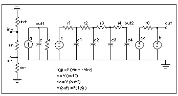
The µA741 op-amp is modeled by PWL controlled sources. The output is limited to ±15 volts by a piecewise linear CCVS (source "h").
0p_amp.sp --- operational amplifier
*
.options post=2
.tran .001ms 2ms
.ac dec 10 .1hz 10me'
*.graph tran vout=v(output)
*.graph tran vin=v(input)
*.graph ac model=grap voutdb=vdb(output)
*.graph ac model=grap vphase=vp(output)
.probe tran vout=v(output) vin=v(input)
.probe ac voutdb=vdb(output) vphase=vp(output)
.model grap plot xscal=2
xamp input 0 output opamp
vin input 0 sin(0,1m,1k) ac 1
* subcircuit definitions
* input subckt
.subckt opin in+ in- out
rin in+ in- 2meg
rin+ in+ 0 500meg
rin- in- 0 500meg
g 0 out pwl(1) in+ in- -68mv,-68ma 68mv,68ma delta=1mv
c out 0 .136uf
r out 0 835k
.ends
.subckt oprc in out
e out1 0 in 0 1
r1 out1 out2 168
r2 out2 out3 1.68k
r3 out3 out4 16.8k
r4 out4 out 168k
c1 out2 0 100p
c2 out3 0 10p
c3 out4 0 1p
c4 out 0 .1p
r out 0 1e12
.ends
.subckt opout in out
eo out1 0 in 0 1
ro out1 out 75
vdum out dum 0
h dum 0 pwl(1) vdum delta=.01ma -.1ma,-15v .1ma,15v
.ends
* op-amp subckt
.subckt opamp in+ in- out
xin in+ in- out1 opin
xrc out1 out2 oprc
xout out2 out opout
.ends
.end
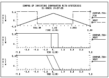
An inverting comparator is modelled by a piecewise linear VCVS.
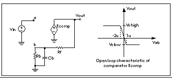
Two reference voltages corresponding to volow and vohigh of Ecomp characteristic are:
When Vin exceeds Vrefhigh, the output Vout goes to Volow. For Vin less than Vreflow, the output goes to Vohigh.
Compar.sp Inverting comparator with hysterisis
.OPTIONS POST PROBE
.PARAM vohigh=5v volow=-2.5v rbval=1k rfval=9k
Ecomp out 0 PWL(1) a b -2u,vohigh 1u,volow
Rb b 0 rbval
Rf b out rfval
Cb b 0 1ff
Vin a 0 PWL(0,-4 1u,4 2u,-4)
.TRAN .1n 2u
.PROBE Vin=V(a) Vab=V(a,b) Vout=V(out)
.END
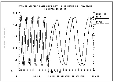
In this example, a one-input NAND functioning as an inverter models a five stage ring oscillator. PWL capacitance is used to switch the load capacitance of this inverter from 1pF to 3 pF. As the simulation results indicate, the oscillation frequency decreases as the load capacitance increases.
vcob.sp voltage controlled oscillator using pwl functions
.OPTION POST
.GLOBAL ctrl
.TRAN 1n 100n
.IC V(in)=0 V(out1)=5
.PROBE TRAN V(in) V(out1) V(out2) V(out3) V(out4)
X1 in out1 inv
X2 out1 out2 inv
X3 out2 out3 inv
X4 out3 out4 inv
X5 out4 in inv
Vctrl ctrl 0 PWL(0,0 35n,0 40n,5)
.SUBCKT inv in out rout=1k
* The following G Element is functioning as PWL capacitance.
Gcout out 0 VCCAP PWL(1) ctrl 0 DELTA=.01
+ 4.5 1p
+ 4.6 3p
Rout out 0 rout
Gn 0 out NAND(1) in 0 SCALE='1.0k/rout'
+ 0. 5.00ma
+ 0.25 4.95ma
+ 0.5 4.85ma
+ 1.0 4.75ma
+ 1.5 4.42ma
+ 3.5 1.00ma
+ 4.000 0.50ma
+ 4.5 0.20ma
+ 5.0 0.05ma
.ENDS inv
*
.END
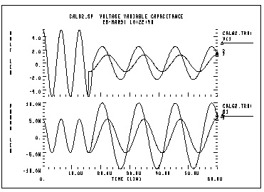
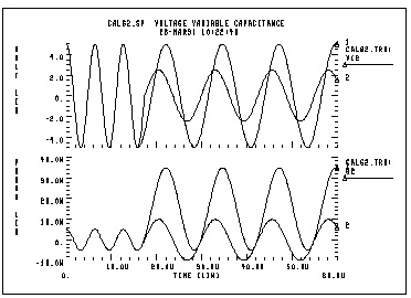
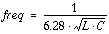
The capacitor is initially charged to 5 volts. The value of capacitance is the function of voltage at node 10. The value of capacitance becomes four times higher at time t2. The frequency of this LC circuit is given by:
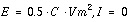
At time t2, the frequency must be halved. The amplitude of oscillation depends on the condition of the circuit when the capacitance value changes. The stored energy is:
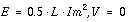
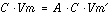
Assuming at time t2, when V=0, C changes to A · C, then:
The second condition to consider is when V=Vin, C changes to A· C. In this case:
Therefore, the voltage amplitude is modified between Vm/sqrt(A) and Vm/A depending on the circuit condition at the switching time. This example tests the CTYPE 0 and 1 results. The result for CTYPE=1 must be correct because capacitance is a function of voltage at node 10, not a function of the voltage across the capacitor itself.
calg2.sp voltage variable capacitance
*
.OPTION POST
.IC v(1)=5 v(2)=5
C1 1 0 C='1e-9*V(10)' CTYPE=1
L1 1 0 1m
*
C2 2 0 C='1e-9*V(10)' CTYPE=0
L2 2 0 1m
*
V10 10 0 PWL(0sec,1v t1,1v t2,4v)
R10 10 0 1
*
.TRAN .1u 60u UIC SWEEP DATA=par
.MEAS TRAN period1 TRIG V(1) VAL=0 RISE=1
+ TARG V(1) VAL=0 RISE=2
.MEAS TRAN period2 TRIG V(1) VAL=0 RISE=5
+ TARG V(1) VAL=0 RISE=6
.PROBE TRAN V(1) q1=LX0(C1)
*
.PROBE TRAN V(2) q2=LX0(C2)
.DATA par t1 t2
15.65us 15.80us
17.30us 17.45us
.ENDDATA
.END