The following components are examples of analog behavioral building blocks. Each demonstrates a basic Star-Hspice feature:
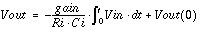
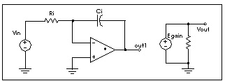
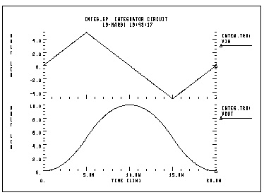
The integrator circuit is modelled by an ideal op-amp and uses a VCVS to adjust the output voltage. The output of integrator is given by:
Integ.sp integrator circuit
.TRAN 1n 20n
.OPTIONS POST PROBE DELMAX =.1n
.PROBE Vin=V(in) Vout=V(out)
.SUBCKT integ in out gain=-1 rval=1k cval=1p
EOP out1 0 OPAMP in- 0
Ri in in- rval
Ci in- out1 cval
Egain out 0 out1 0 gain
Rout out 0 1e12
.ENDS
Xint in out integ gain=-0.4
Vin in 0 PWL(0,0 5n,5v 15n,-5v 20n,0)
.END
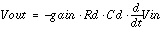
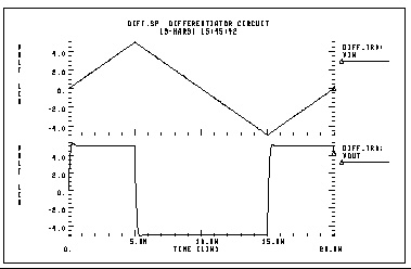
A differentiator is modelled by an ideal op-amp and a VCVS for adjusting the magnitude and polarity of the output. The differentiator response is given by:
For a high-frequency signal, the output of a differentiator can have overshoot at the edges. You can smooth this out using a simple RC filter.
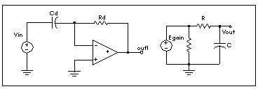
Diff.sp differentiator circuit
* V(out)=Rval * Cval * gain * (dV(in)/dt)
.TRAN 1n 20n
.PROBE Vin=V(in) Vout=V(out)
.OPTIONS PROBE POST
.SUBCKT diff in out gain=-1 rval=1k cval=1pf
EOP out1 0 OPAMP in- 0
Cd in in- cval
Rd in- out1 rval
Egain out2 0 out1 0 gain
Rout out2 0 1e12
*rc filter to smooth the output
R out2 out 75
C out 0 1pf
.ENDS
Xdiff in out diff rval=5k
Vin in 0 PWL(0,0 5n,5v 15n,-5v 20n,0)
.END
The following example uses the ideal transformer to convert 8 ohms impedance of a loudspeaker to 800 ohms impedance, which is a proper load value for a power amplifier, Rin=n
MATCHING IMPEDANCE BY USING IDEAL TRANSFORMER
E OUT 0 TRANSFORMER IN 0 10
RL OUT 0 8
VIN IN 0 1
.OP
.END
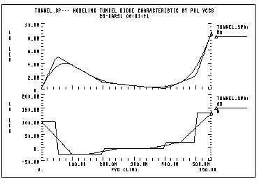
In the following example, a tunnel diode is modeled by a PWL VCCS. The current characteristics are obtained for two DELTA values (50 µv and 10 µv). The IV characteristics corresponding to DELTA=10 µv have sharper corners. The derivative of current with respect to voltage (GD) is also displayed. The GD value around breakpoints changes in a linear fashion.
tunnel.sp-- modeling tunnel diode characteristic by pwl vccs
* pwl function is tested for two different delta values. The
* smaller delta will create the sharper corners.
.options post=2
vin 1 0 pvd
.dc pvd 0 550m 5m sweep delta poi 2 50mv 5mv
.probe dc id=lx0(g) gd=lx2(g)
g 1 0 pwl(1) 1 0 delta=delta
+ -50mv,-5ma 50mv,5ma 200mv,1ma 400mv,.05ma
+ 500mv,2ma 600mv,15ma
.end
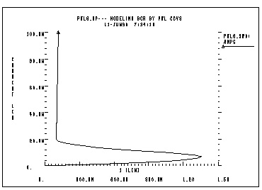
The silicon controlled rectifier (SCR) characteristic can be easily modeled using a PWL CCVS because there is a unique voltage value for any current value.
pwl6.sp--- modeling SCR by pwl ccvs
*The silicon controlled rectifier (SCR) characteristic
*is modelled by a piecewise linear current controlled
*voltage source (PWL_CCVS), because for any current value
*there is a unique voltage value.
*
*use iscr as y-axis and v(1) as x-axis
*
.options post=2
iscr 0 2 0
vdum 2 1 0
.dc iscr 0 1u 1n
.probe vscr=lx0(h) transr=lx3(h)
h 1 0 pwl(1) vdum -5na,-2v 5na,2v 15na,.1v 1ua,.3v 10ua,.5
+ delta=5na
.end
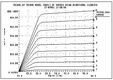
The following example shows how to include the behavioral elements in a subcircuit to give very good triode tube action. The basic power law equation (current source gt) is modified by the voltage source ea to give better response in saturation.
triode.sp triode model family of curves using behavioral elements
.options post acct
.dc va 20v 60v 1v vg 1v 10v 1v
.probe ianode=i(xt.ra) v(anode) v(grid) eqn=lv6(xt.gt)
.print v(xt.int_anode) v(xt.i_anode) inode=i(xt.ra) eqn=lv6(xt.gt)
vg grid 0 1v
va anode 0 20v
vc cathode 0 0v
xt anode grid cathode triode
.subckt triode anode grid cathode
* 5 ohm anode resistance
* ea creates saturation region conductance
ra anode i_anode 5
ea int_anode cathode pwl(1) i_anode cathode delta=.01
+ 20,0 27,.85 28,.95 29,.99 30,1 130,1.2
gt i_anode cathode
+ cur='20m*v(int_anode,cathode)*pwr(max(v(grid,cathode),0),1.5)'
cga grid i_anode 30p
cgc grid cathode 20p
cac i_anode cathode 5p
.ends
*
.end
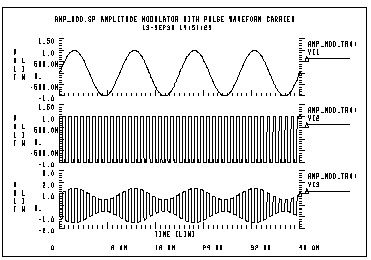
This example uses a G Element as an amplitude modulator with pulse waveform carrier.
amp_mod.sp amplitude modulator with pulse waveform carrier
.OPTIONS POST
.TRAN .05m 40m
.PROBE V(1) V(2) V(3)
Vs 1 0 SIN(0,1,100)
Vc 2 0 PULSE(1,-1,0,1n,1n,.5m,1m)
Rs 1 0 1+
Rc 2 0 1
G 0 3 CUR='(1+.5*V(1))*V(2)'
Re 3 0 1
.END
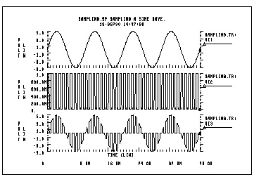
A behavioral data sample follows.
sampling.sp sampling a sine wave.
.OPTIONS POST
.TRAN .05m 40m
.PROBE V(1) V(2) V(3)
Vc 1 0 SIN(0,5,100)
Vs 2 0 PULSE(0,1,0,1n,1n,.5m,1m)
Rc 1 0 1
Rs 2 0 1
E 3 0 VOL='V(1)*V(2)'
Re 3 0 1
.END