This section describes how to calibrate with digital behavioral components.
The following simulation demonstrates an ACL family output buffer with 2 ns delay and 1.8 ns rise and fall time. The ground and VDD supply currents and the internal ground bounce due to the package are also shown.
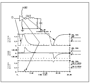
Star-Hspice can automatically measure the datasheet quantities such as TPHL, risetime, maximum power dissipation, and ground bounce using the following commands.
.MEAS tphl trig v(D) val='.5*vdd' rise=1
+ targ v(out) val='.5*vdd' fall=1
.MEAS risetime trig v(out) val='.1*vdd' rise=1
+ targ v(out) val='.9*vdd' rise=1
.MEAS max_power max power
.MEAS bounce max v(xin.v_local)
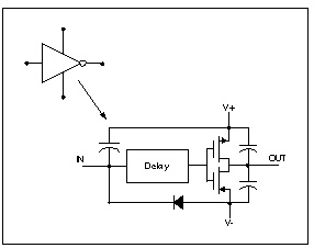
The inverter is composed of capacitors, diodes, one-dimensional lookup table MOSFETs, and a special low-pass delay element. The low-pass delay element has the property that attenuates pulses that are narrower than the delay value.
.subckt inv in out v+ v-
cout+ out_l v+ 2p
cout- out_l v- 2p
xmp out_l inx v+ pmos
xmn out_l inx v- nmos
e inx v- delay in v- td=1n
din v- in dx
.model dx d cjo=2pf
chi in v+ .5pf
.ends inv
The behavioral MOSFETs are represented by one dimensional lookup tables. The equivalent n-channel lookup table is shown below.
.subckt nmos 1 2 3
gn 3 1 VCR npwl(1) 2 3 scale=0.008
* VOLTAGE RESISTANCE
+ 0. 495.8840g
+ 200.00000m 456.0938g
+ 400.00000m 141.6902g
+ 600.00000m 7.0624g
+ 800.00000m 258.9313meg
+ 1.00000 6.4866meg
+ 1.20000 842.9467k
+ 1.40000 21.6882k
+ 1.60000 170.8367k
+ 1.80000 106.4944k
+ 2.00000 72.7598k
+ 2.20000 52.4632k
+ 2.40000 38.5634k
+ 2.60000 8.8056k
+ 2.80000 5.2543k
+ 3.00000 4.3553k
+ 3.40000 3.4950k
+ 3.80000 2.0534k
+ 4.20000 2.7852k
+ 4.60000 2.5k
+ 5.0 2.3k
.ends nmos
The table above describes a voltage versus resistance table. It shows, for example, that the resistance at 5 volts is 2.3 kohm.
You can create an inverter lookup table in two simple steps. First simulate an actual transistor level inverter using a DC sweep of the input and print the output V/I for the output pullup and pulldown transistors. Next, copy the printed output into the volt controlled resistor lookup table element.
The following test file, inv_vin_vout.sp calculates RN (the effective pulldown resistor transfer function) and RP (the pullup transfer function).
RN is calculated as Vout/I(mn) where mn is the pulldown transistor. RP is calculated as (VCC-Vout)/I(mp) where mp is the pullup transfer function.
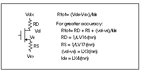
The actual calculation uses a more accurate way of obtaining the transistor series resistance as follows:
The first graph below shows VIN versus VOUT and the second graph shows the computed transfer resistances RP and RN as a function of VIN.
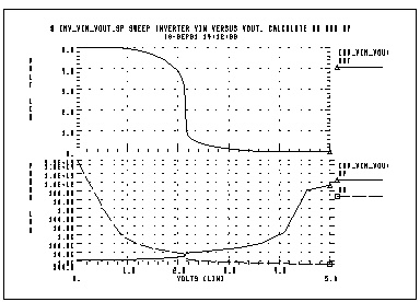
The Star-Hspice file used to calculate RP and RN is
$ inv_vin_vout.sp sweep inverter vin versus vout, calculate rn and rp
The triple range DC sweep allows coarse grid before and after:
* use dc sweep with 3 ranges; 0-1.5v, 1.6-2.5, 2.6 5
.dc vin lin 8 0 2.0 lin 20 2.1 2.5 lin 6 2.75 5
$$ rn=par(`v(out)/i(x1.mn)')
.print rn=
+ par(`1/lv16(x1.mn)+1/lv17(x1.mn)+abs(lx3(x1.mn)/lx4(x1.mn))')
.print rp=par(`(-vcc+v(out))/i(x1.mp)')
.param sigma=0 vcc=5
.global vcc
vcc vcc 0 vcc
vin in 0 pwl 0,0 0.2n,5
x1 in out inv
.macro inv in out
mn out in 0 0 nch w=10u l=1u
mp out in vcc vcc pch w=10u l=1u
.eom
The tabular listing produced by Star-Hspice is
****** dc transfer curves tnom= 25.000 temp= 25.000
******
volt rn
0. 3.312e+14
285.71429m 317.3503g
571.42857m 304.0682x
857.14286m 1.1222x
1.14286 107.6844k
1.42857 32.1373k
1.71429 14.6984k
2.00000 7.7108k
2.10000 5.8210k
2.12105 5.1059k
2.14211 3.2036k
2.16316 1.6906k
2.18421 1.4421k
2.20526 1.3255k
2.22632 1.2470k
2.24737 1.1860k
2.26842 1.1360k
2.28947 1.0935k
2.31053 1.0565k
2.33158 1.0238k
2.35263 994.3804
2.37368 967.7559
2.39474 943.4266
2.41579 921.0413
2.43684 900.3251
2.45789 881.0585
2.47895 863.0632
2.50000 846.1922
2.75000 701.5119
3.20000 560.6908
3.65000 479.8893
4.10000 426.4486
4.55000 387.7524
5.00000 357.4228
Calibrate behavioral models by running Star-Hspice on the full transistor version of a cell and then optimizing the behavioral model to this data.
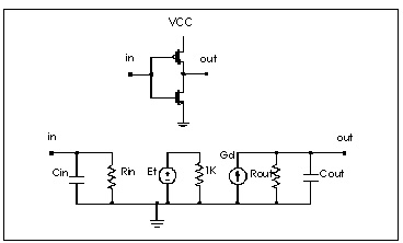
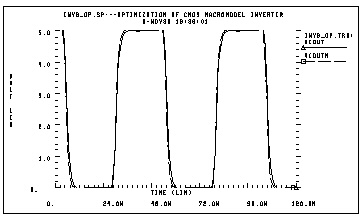
In this example, Star-Hspice simulates the CMOS inverter using the LEVEL 3 MOSFET model. The input and output resistances are obtained by performing a .TF transfer function analysis (.TF V(out) Vin). The transfer function table of the inverter is obtained by performing the .DC analysis sweeping input voltage (.DC Vin 0 5 .1). This table is then used in the PWL element to represent the transfer function of the inverter. The rise and fall time of the inverter in the equivalent circuit is adjusted by a voltage controlled PWL capacitance across the output resistance. The propagation delay is obtained by the delay element across the output rc circuit. The input capacitance is adjusted by using the inverter in a ring oscillator. All the adjustment in this example is done using the Star-Hspice optimization analysis. The data file and the results are shown below.
INVB_OP.SP---OPTIMIZATION OF CMOS MACROMODEL INVERTER
.OPTIONS POST PROBE NOMOD METHOD=GEAR
.GLOBAL VCC VCCM
.PARAM VCC=5 ROUT=2.5K CAPIN=.5P
+ TDELAY=OPTINV(1.0N,.5N,3N)
+ CAPL=OPTINV(.2P,.1P,.6P)
+ CAPH=OPTINV(.2P,.1P,.6P)
.TRAN .25N 120NS
+ SWEEP OPTIMIZE=OPTINV RESULTS=RISEX,FALLX,PROPFX,PROPRX
+ MODEL=OPT1
.MODEL OPT1 OPT ITROPT=30 RELIN=1.0E-5 RELOUT=1E-4
.MEAS TRAN PROPFM TRIG V(INM) VAL='.5*VCC' RISE=2
+ TARG V(OUTM) VAL='.5*VCC' FALL=2
.MEAS TRAN PROPFX TRIG V(IN) VAL='.5*VCC' RISE=2
+ TARG V(OUT) VAL='.5*VCC' FALL=2
+ GOAL='PROPFM' WEIGHT=0.8
.MEAS TRAN PROPRM TRIG V(INM) VAL='.5*VCC' FALL=2
+ TARG V(OUTM) VAL='.5*VCC' RISE=2
.MEAS TRAN PROPRX TRIG V(IN) VAL='.5*VCC' FALL=2
+ TARG V(OUT) VAL='.5*VCC' RISE=2
+ GOAL='PROPRM' WEIGHT=0.8
.MEAS TRAN FALLM TRIG V(OUTM) VAL='.9*VCC' FALL=2
+ TARG V(OUTM) VAL='.1*VCC' FALL=2
.MEAS TRAN FALLX TRIG V(OUT) VAL='.9*VCC' FALL=2
+ TARG V(OUT) VAL='.1*VCC' FALL=2
+ GOAL='FALLM'
.MEAS TRAN RISEM TRIG V(OUTM) VAL='.1*VCC' RISE=2
+ TARG V(OUTM) VAL='.9*VCC' RISE=2
.MEAS TRAN RISEX TRIG V(OUT) VAL='.1*VCC' RISE=2
+ TARG V(OUT) VAL='.9*VCC' RISE=2
+ GOAL='RISEM'
.TRAN 0.5N 120N
.PROBE V(out) V(outm)
VC VCC 0 VCC
VCCM VCCM 0 VCC
X1 IN OUT INV
X1M INM OUTM INVM
VIN IN GND PULSE(0,5 1N,5N,5N 20N,50N)
VINM INM GND PULSE(0,5 1N,5N,5N 20N,50N)
.SUBCKT INV IN OUT
RIN IN 0 1E12
CIN IN 0 CAPIN
ET 1 0 PWL(1) IN 0
+ 1.00000 5.0
+ 1.50000 4.93
+ 2.00000 4.72
+ 2.40000 4.21
+ 2.50000 3.77
+ 2.60000 0.90
+ 2.70000 0.65
+ 3.00000 0.30
+ 3.50000 0.092
+ 4.00000 0.006
+ 4.60000 0.
RT 1 0 1K
GD 0 OUT DELAY 1 0 TD=TDELAY SCALE='1/ROUT'
GCOUT OUT 0 VCCAP PWL(1) IN 0 1V,CAPL 2V,CAPH
ROUT OUT 0 ROUT
.ENDS
.SUBCKT INVM IN OUT
XP1 OUT IN VCCM VCCM MP
XN1 OUT IN GND GND MN
.ENDS
.MODEL N NMOS LEVEL=3 TOX=850E-10 LD=.85U NSUB=2E16 VTO=1
+ GAMMA=1.4 PHI=.9 UO=823 VMAX=2.7E5 XJ=0.9U KAPPA=1.6
+ ETA=.1 THETA=.18 NFS=1.6E11 RSH=25 CJ=1.85E-4 MJ=.42 PB=.7
+ CJSW=6.2E-10 MJSW=.34 CGSO=5.3E-10 CGDO=5.3E-10
+ CGBO=1.75E-9
.MODEL P PMOS LEVEL=3 TOX=850E-10 LD=.6U
+ NSUB=1.4E16 VTO=-.86 GAMMA=.65 PHI=.76 UO=266
+ VMAX=.8E5 XJ=0.7U KAPPA=4 ETA=.25 THETA=.08 NFS=2.3E11
+ RSH=85 CJ=1.78E-4 MJ=.4 PB=.6 CJSW=5E-10 MJSW=.22
+ CGSO=5.3E-10 CGDO=5.3E-10 CGBO=.98E-9
SUBCKT MP 1 2 3 4
M1 1 2 3 4 P W=45U L=5U AD=615P AS=615P
+ PD=65U PS=65U NRD=.4 NRS=.4
.ENDS MP
.SUBCKT MN 1 2 3 4
M1 1 2 3 4 N W=17U L=5U AD=440P AS=440P
+ PD=80U PS=80U NRD=.85 NRS=.85
.ENDS MN
.END
OPTIMIZATION RESULTS
RESIDUAL SUM OF SQUARES = 4.589123E-03
NORM OF THE GRADIENT = 1.155285E-04
MARQUARDT SCALING PARAMETER = 130.602
NO. OF FUNCTION EVALUATIONS = 51
NO. OF ITERATIONS = 15
OPTIMIZATION COMPLETED
MEASURED RESULTS < RELOUT= 1.0000E-04 ON LAST ITERATIONS
* %NORM-SEN %CHANGE
.PARAM TDELAY = 1.3251N $ 37.6164 -48.6429U
.PARAM CAPL = 390.2613F $ 37.2396 60.2596U
.PARAM CAPH = 364.2716F $ 25.1440 62.1922U
* RISEX = 2.7018N
* FALLX = 2.5388N
* PROPFX = 2.0738N
* PROPRX = 2.1107N
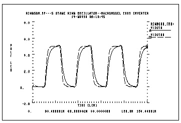
To optimize behavioral ring oscillator performance, review the examples in this section.
RING5BM.SP-5 STAGE RING OSCILLATOR--MACROMODEL CMOS INVERTER
.IC V(IN)=5 V(OUT1)=0 V(OUT2)=5 V(OUT3)=0
.IC V(INM)=5 V(OUT1M)=0 V(OUT2M)=5 V(OUT3M)=0
.GLOBAL VCCM
.OPTIONS NOMOD POST=2 PROBE METHOD=GEAR DELMAX=0.5N
.PARAM VCC=5 $ CAPIN=0.92137P
.PARAM TDELAY=1.32N CAPL=390.26F CAPH=364.27F ROUT=2.5K
+ CAPIN=OPTOSC(0.8P,0.1P,1.0P)
.TRAN 1NS 150NS UIC
+ SWEEP OPTIMIZE=OPTOSC RESULTS=PERIODX MODEL=OPT1
.MODEL OPT1 OPT RELIN=1E-5 RELOUT=1E-4 DIFSIZ=.02 ITROPT=25
.MEAS TRAN PERIODM TRIG V(OUT3M) VAL='.8*VCC' RISE=2
+ TARG V(OUT3M) VAL='.8*VCC' RISE=3
.MEAS TRAN PERIODX TRIG V(OUT3) VAL='.8*VCC' RISE=2
+ TARG V(OUT3) VAL='.8*VCC' RISE=3
+ GOAL='PERIODM'
.TRAN 1NS 150NS UIC
.PROBE V(OUT3) V(OUT3M)
X1 IN OUT1 INV
X2 OUT1 OUT2 INV
X3 OUT2 OUT3 INV
X4 OUT3 OUT4 INV
X5 OUT4 IN INV
CL IN 0 1P
VCCM VCCM 0 VCC
X1M INM OUT1M INVM
X2M OUT1M OUT2M INVM
X3M OUT2M OUT3M INVM
X4M OUT3M OUT4M INVM
X5M OUT4M INM INVM
CLM INM 0 1P
*Subcircuit definitions given in the previous example are not repeated here.
.END
Optimization Results
RESIDUAL SUM OF SQUARES = 4.704516E-10
NORM OF THE GRADIENT = 2.887249E-04
MARQUARDT SCALING PARAMETER = 32.0000
NO. OF FUNCTION EVALUATIONS = 52
NO. OF ITERATIONS = 20
OTIMIZATION COMPLETED
MEASURED RESULTS < RELOUT= 1.0000E-04 ON LAST ITERATIONS
**** OPTIMIZED PARAMETERS OPTOSC
* %NORM-SEN %CHANGE
.PARAM CAPIN = 921.4155F $ 100.0000 8.5740U
*** OPTIMIZE RESULTS MEASURE NAMES AND VALUES
* PERIODX = 40.3180N