This section provides example of how to model with digital behavioral components.
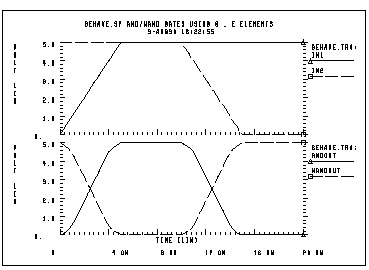
In this example, a two-input AND gate is modeled by a G Element. A two-input NAND gate is modeled by an E Element.
behave.sp and/nand gates using g, e Elements
.options post=2
.op
.tran .5n 20n
.probe v(in1) v(in2) v(andout) v(in1) v(in2) v(nandout)
g 0 andout and(2) in1 0 in2 0
+ 0.0 0.0ma
+ 0.5 0.1ma
+ 1.0 0.5ma
+ 4.0 4.5ma
+ 4.5 4.8ma
+ 5.0 5.0ma
*
e nandout 0 nand(2) in1 0 in2 0
+ 0.0 5.0v
+ 0.5 4.8v
+ 1.0 4.5v
+ 4.0 0.5v
+ 4.5 0.2v
+ 5.0 0.0v
*
vin1 in1 0 0 pwl(0,0 5ns,5)
vin2 in2 0 5 pwl(0,5 10ns,5 15ns,0)
rin1 in1 0 1k
rin2 in2 0 1k
rand andout 0 1k
rnand nandout 0 1k
.end
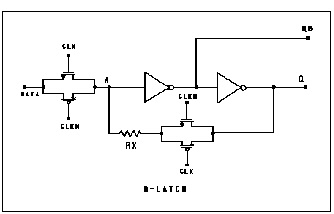
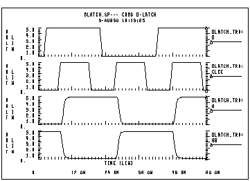
In this example, a D flip-flop is modeled by one input NAND gates and NPWL/PPWL functions.
dlatch.sp--- cmos d-latch
.option post
.tran .2n 60ns
.probe tran clock=v(clck)data=v(d) q=v(q)
.ic v(q)=0
vdata d 0 pulse(0,5 2n,1n,1n 19n,40n)
vclk clck 0 pulse(0,5 7n,1n,1n 10n,20n)
vclkn clckn 0 pulse(5,0 7n,1n,1n 10n,20n)
xdlatch d clck clckn q qb dlatch cinv=.2p
* DRAIN GATE SOURCE
.SUBCKT nmos 1 2 3 capm=.5p
cd 1 0 capm
cs 3 0 capm
gn 3 1 VCR NPWL(1) 2 3
+ 0. 495.8840G
+ 200.00000M 456.0938G
+ 400.00000M 141.6902G
+ 600.00000M 7.0624G
+ 800.00000M 258.9313X
+ 1.00000 6.4866X
+ 1.20000 842.9467K
+ 1.40000 321.6882K
+ 1.60000 170.8367K
+ 1.80000 106.4944K
+ 2.00000 72.7598K
+ 2.20000 52.4632K
+ 2.40000 38.5634K
+ 2.60000 8.8056K
+ 2.80000 5.2543K
+ 3.00000 4.3553K
+ 3.20000 3.8407K
+ 3.40000 3.4950K
+ 3.60000 3.2441K
+ 3.80000 3.0534K
+ 4.00000 2.9042K
+ 4.20000 2.7852K
+ 4.40000 2.6822K
+ 4.60000 2.5k
+ 5.0 2.3k
.ENDS nmos
* DRAIN GATE SOURCE
.SUBCKT pmos 1 2 3 capm=.5p
cd 1 0 capm
cs 3 0 capm
gp 1 3 VCR PPWL(1) 2 3
+ -5.0000 2.3845K
+ -4.8000 2.4733K
+ -4.6000 2.5719K
+ -4.4000 2.6813K
+ -4.2000 2.8035K
+ -4.0000 2.9415K
+ -3.8000 3.1116K
+ -3.6000 3.3221K
+ -3.4000 3.5895K
+ -3.2000 3.9410K
+ -3.0000 4.4288K
+ -2.8000 5.1745K
+ -2.6000 6.6041K
+ -2.4000 29.6203K
+ -2.2000 42.4517K
+ -2.0000 58.3239K
+ -1.8000 83.4296K
+ -1.6000 128.1517K
+ -1.4000 221.2640K
+ -1.2000 471.8433K
+ -1.0000 1.6359X
+ -800.00M 41.7023X
+ -600.00M 1.3394G
+ -400.00M 38.3449G
+ -200.00M 267.7325G
+ 0. 328.7122G
.ENDS pmos
*
.subckt tgate in out clk clkn ctg=.5p
xmn in clk out nmos capm=ctg
xmp in clkn out pmos capm=ctg
.ends tgate
.SUBCKT inv in out capout=1p
cout out 0 capout
rout out 0 1.0k
gn 0 out nand(1) in 0 scale=1
+ 0. 4.90ma
+ 0.25 4.88ma
+ 0.5 4.85ma
+ 1.0 4.75ma
+ 1.5 4.42ma
+ 3.5 1.00ma
+ 4.000 0.50ma
+ 4.5 0.2ma
+ 5.0 0.1ma
.ENDS inv
.subckt dlatch data clck clckn q qb cinv=1p
xtg1 data a clck clckn tgate ctg='cinv/2'
xtg2 q ax clckn clck tgate ctg='cinv/2'
rx ax a 5
xinv1 a qb inv capout=cinv
xinv2 qb q inv capout=cinv
.ends dlatch
.end
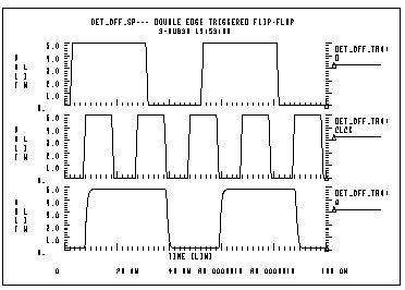
In this example a double edged triggered flip-flop is modeled by using the D_LATCH subcircuit from previous example and several NAND gates.
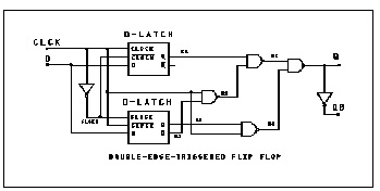
det_dff.sp--- double edge triggered flip-flop
.option post=2
.tran .2n 100ns
.probe tran clock=v(clck) data=v(d) q=v(q)
vdata d 0 pulse(0,5 2n,1n,1n 28n,50n)
vclk clck 0 pulse(0,5 7n,1n,1n 10n,20n)
xclkn clck clckn inv cinv=.1p
xd1 d clck clckn q1 qb1 dlatch cinv=.2p
xd2 d clckn clck q2 qb2 dlatch cinv=.2p
xnand1 clck qb2 n1 nand2 capout=.5p
xnand2 q1 n1 n2 nand2 capout=.5p
xnand3 q2 clck n3 nand2 capout=.5p
xnand4 n2 n3 q nand2 capout=.5p
xinv q qb inv capout=.5p
*Note: Subcircuit definitions for NMOS, PMOS, and INV are given in the
* D-Latch examples; therefore they are not repeated here.
*
.SUBCKT nand2 in1 in2 out capout=2p
cout out 0 capout
rout out 0 1.0k
gn 0 out nand(2) in1 0 in2 0 scale=1
+ 0. 4.90ma
+ 0.25 4.88ma
+ 0.5 4.85ma
+ 1.0 4.75ma
+ 1.5 4.42ma
+ 3.5 1.00ma
+ 4.000 0.50ma
+ 4.5 0.2ma
+ 5.0 0.1ma
.ENDS nand2
*
.subckt dlatch data clck clckn q qb cinv=1p
xtg1 data a clck clckn tgate ctg='cinv/2'
xtg2 q ax clckn clck tgate ctg='cinv/2'
rx ax a 10
xinv1 a qb inv capout=cinv
xinv2 qb q inv capout=cinv
.ends dlatch
.end