LEVEL 27 SOSFET Model
A three-terminal silicon-on-sapphire (SOS) FET transistor model is available in Star-Hspice
Fargher, H. E. and Mole, P. J. The Implementation Of A 3 Terminal SOSFET Model In SPICE For Circuit Simulation. GEC VLSI Research Laboratory, MOS1 Division.
. This SOSFET model is based on a sapphire insulator that isolates the substrate and models the behavior of SOS devices more accurately than standard MOSFET models with physically unreal parameter values. The SOSFET model also includes a charge conservation model (Ward and Dutton model based).
Because the defaults of the SOSFET model parameters are channel-length dependent, you must specify the model parameter SOSLEV to select either the 5 µm or 3 µm processing model.
Setting SOSLEV=1 selects the 5 µm model; otherwise the 3 µm model is automatically set, including the second-order effects (default=3 µm).
NOTE: There is no bulk node specification for this model. If bulk nodes are specified, Star-Hspice ignores them.
This model does not use the model parameter ACM because the model includes no junction diodes. Also, the model parameter CAPOP only accepts a value of 7. Seven is its own charge conservation model, which cannot be used by the other level MOSFET models.
Temperature compensation equations for SOSFET model parameters VTO and UO are the same as those used for the MOSFET model.
NOTE: The model provides a special option for bulk nodes for silicon on sapphire. In the model definition, when you specify -1 for the bulk node, the model generates a special node for each element. This bulk node is named in the form, B#<element name>, where the element name is that of the defined element. Use this name in any statement, such as a .PRINT statement, to refer to the element's bulk node.
Syntax
.MODEL mname PMOS <LEVEL=27> <SOSLEV=val> <pname1=val1>...
or
.MODEL mname NMOS <LEVEL=27> <SOSLEV=val> <pname=val1>...
|
mname
|
The model name
|
|
PMOS
|
Identifies a p-channel MOSFET model
|
|
NMOS
|
Identifies an n-channel MOSFET model
|
|
LEVEL
|
Model level selector
|
|
SOSLEV
|
Selects the processing model. If you set SOSLEV=1, the default=5µm. The automatic default=3µm.
|
|
pname
|
Parameter model
|
LEVEL 27 Model Parameters
5-µm Model Parameters
|
Name (Alias)
|
Units
|
Default
|
Description
|
|
CGDO
|
F/m
|
|
Gate-drain overlap capacitance per unit channel width. The default=3.1e-10 (n-type), 2.2e-10 (p-type).
|
|
CGSO
|
F/m
|
|
Gate-source overlap capacitance per unit channel width. The default=3.1e-10 (n-type), 2.2e-10 (p-type).
|
|
LD
|
m
|
|
Lateral diffusion. The default=0.6µ (n- type), 0.3µ (p-type).
|
|
RSH
|
ohm/sq
|
|
Drain and source diffusion sheet resistance. The default=25 (n-type), 100 (p-type).
|
|
SOSLEV
|
|
1
|
Model index
|
|
TOX
|
m
|
7.0e-8
|
Oxide thickness
|
|
UO
|
cm
2
/(V·s)
|
|
Surface mobility. The default=350 (n-type), 220 (p-type).
|
|
VTO
|
V
|
|
Threshold voltage. The default=1.25 (n-type), -1.25 (p-type).
|
3-µm Model Parameters
|
Name (Alias)
|
Units
|
Default
|
Description
|
|
A
|
m/V
|
0.1µm
|
Channel length shortening coefficient (2nd effect)
|
|
ALPHA
|
V/m
|
|
Threshold voltage length dependence. The default=0.15µ (n-type), 0.18µ (p-type).
|
|
CAPOP
|
|
7
|
Capacitance model selector
|
|
CGDO
|
F/m
|
|
Gate-drain overlap capacitance per unit channel width. The default=4.6e-10 (n-type), 3.6e-10 (p-type).
|
|
CGSO
|
F/m
|
|
Gate-source overlap capacitance per unit channel width. The default=4.6e-10 (n-type), 3.6e-10 (p-type).
|
|
EC
|
V/m
|
|
Critical electric field for velocity saturation (2nd effect). The default=3.0e6 (n-type), 7.5e6 (p-type).
|
|
FB
|
|
|
Body effect coefficient (2nd effect). The default=0.15 (n-type), 0 (p-type).
|
|
LD
|
m
|
|
Lateral diffusion. The default=0.3µ (n-type), 0.2µ (p-type).
|
|
LEVEL
|
|
27
|
Model level selector
|
|
RSH
|
ohm/sq
|
|
Drain and source diffusion sheet resistance. The default=25
(n-type), 80 (p-type).
|
|
SOSLEV
|
|
2
|
Model index
|
|
THETA
|
1/V
|
|
Mobility degradation coefficient (2nd effect). The default=0.055 (n-type), 0.075 (p-type).
|
|
TOX
|
m
|
3.4e-8
|
Oxide thickness
|
|
UO
|
cm
2
/(V·s)
|
|
Surface mobility. The default=370 (n-type), 215 (p-type).
|
|
VTO
|
V
|
|
Threshold voltage. The default=0.83 (n-type), -0.74 (p-type).
|
Example
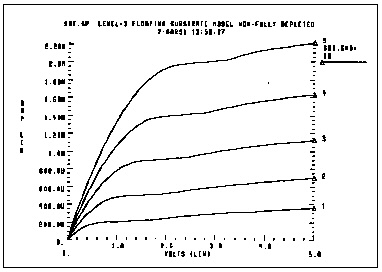
*FILE ML27IV.SP: IDS AND VGS CURVES FOR NMOS AND PMOS SOSFETS.
.OPTIONS ACCT LIST NOPAGE NOMOD
.OP
.DC VDDN 0 5.0 .1
* N-CHANNEL IDS CURVES (VD=0->5, VG=1,2,3,4,5)
.PRINT DC I(VN1) I(VN2) I(VN3) I(VN4) I(VN5)
.PLOT DC I(VN1) I(VN2) I(VN3) I(VN4) I(VN5)
* P-CHANNEL IDS CURVES (VD=0->-5,VG=-1,-2,-3,-4,-5)
.PRINT DC I(VP1) I(VP2) I(VP3) I(VP4) I(VP5)
.PLOT DC I(VP1) I(VP2) I(VP3) I(VP4) I(VP5)
* V G S CURVES
.PRINT DC I(VN6) I(VP6)
.PLOT DC I(VN6) I(VP6)
* N-CHANNEL LX7=GM (VD=5, VG=0->5, VS=0)
* N-CHANNEL LX8=GD (VD=0->5, VG=5, VS=0)
* N-CHANNEL LX9=GB (VD=5, VG=5, VS=0)
.PLOT DC LX7 (M21) LX8(M5) LX9(M31)
* P-CHANNEL LX7=GM (VD=0, VG=0->-5, VS=-5)
* P-CHANNEL LX8=GD (VD=0->-5, VG=-5, VS=-5)
* P-CHANNEL LX9=GB (VD=0, VG=0, VS=-5)
.PLOT DC LX7(M22) LX8(M15) LX9(M32)
*
VDDN 99 0 5.0
EPD 98 0 99 0 -1
V1 1 0 1
V2 2 0 2
V3 3 0 3
V4 4 0 4
V5 5 0 5
V11 11 0 -1
V12 12 0 -2
V13 13 0 -3
V14 14 0 -4
V15 15 0 -5
*
VN1 99 31 0
VN2 99 32 0
VN3 99 33 0
VN4 99 34 0
VN5 99 35 0
M1 31 1 0 N1 8U 8U
M2 32 2 0 N1 8U 8U
M3 33 3 0 N1 8U 8U
M4 34 4 0 N1 8U 8U
M5 35 5 0 N1 8U 8U
*
VP1 98 41 0
VP2 98 42 0
VP3 98 43 0
VP4 98 44 0
VP5 98 45 0
M11 41 11 0 P1 8U 8U
M12 42 12 0 P1 8U 8U
M13 43 13 0 P1 8U 8U
M14 44 14 0 P1 8U 8U
M15 45 15 0 P1 8U 8U
*
G M Test
VN6 5 36 0
VP6 0 46 0
M21 36 99 0 N1 8U 8U
M22 46 98 15 P1 8U 8U
*
G M B Test
VN7 5 37 0
VP7 0 47 0
M31 37 5 0 98 N1 8U 8U
M32 47 0 15 99 P1 8U 8U
*
.MODEL N1 NMOS LEVEL=27 SOSLEV=2
+ VTO=0.814 TOX=0.34E-7 THETA=0.55E-1
+ FB=0.15 EC=0.3E7 A=0.1E-6
+ UO=370 CGSO=0.46E-9 CGDO=0.46E-9
+ RSH=25 LD=0.3E-6
*
.MODEL P1 PMOS LEVEL=27 SOSLEV=2
+ VTO=-0.7212 TOX=0.34E-7 THETA=0.75E-1
+ FB=0.0 EC=0.75E7 A=0.1E-6
+ UO=215 CGSO=0.36E-9 CGDO=0.36E-9
+ RSH=80 LD=0.2E-6
*
.END
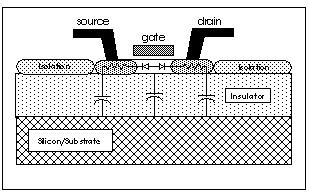
Non-Fully Depleted SOI Model
When using Star-Hspice for SOS/SOI applications, several approaches are currently available. Star-Hspice has a 3-terminal SOS model (LEVEL=27) that is stable for circuit design usage, but has some limitations. The model does not have provisions for depleted bulk. Use it only with non-fully depleted applications and where kink effects are not considered.
The following circuit example is a 4-terminal SOI model for incompletely depleted bulk with kink effect. The example uses a subcircuit to allow a parasitic capacitance to the substrate. In this example, the bulk is considered to be the region under the channel. The substrate is assumed to be the conductive layer under the insulator.
For SOI, the insulator is usually silicon dioxide and the substrate is silicon. For SOS, the insulator is sapphire and the substrate is the metal that contacts the back of the integrated circuit die.
Model Components
The model consists of the following subcomponents:
-
Core IDS model: any level works since the impact ionization and weak inversion models are common to all DC levels. The example uses a LEVEL=3 DC MOS model.
-
Subthreshold model: the model parameter WIC=3 allows the older models to use the more advanced models found in the BSIM (LEVEL=13, LEVEL=28) models. Model parameter N0 should have a typical value around 1.0.
-
Impact ionization model: set the parameters ALPHA and VCR to enable the impact ionization model. Impact ionization is available to all MOS DC equations. Typical values are ALPHA=0.1 and VCR=18.
-
Charge conservation gate cap model (CAPOP=9 XQC=.4) keeps the floating bulk node from obtaining extreme values.
-
The automatic periphery diode area calculation method (ACM) is set to 3 to allow automatic calculation of the source and drain resistances and diode junction leakage and capacitance. (ACM=3 CJ=0 CJSW=0 CJGATE=4e-10 JS=0 JSW=1e-9 LD=.1u HDIF=1.5u RS=40 RD=40 N=1).
NOTE: It is assumed that the source/drain diffusions extend to the buried oxide; thus, the area part of the diode has no capacitance to bulk. Linear capacitors to the substrate, however, are included in the subcircuit.
Obtaining Model Parameters
Use the Star-Hspice optimizing capabilities to obtain the core IDS model parameters.
Use the optimizer to get the core model, subthreshold, and impact ionization parameters. The subthreshold model selected is an improved BSIM type of model that was altered for the older models. The impact ionization model is similar to the Intel model.
The charge conservation model is more charge conserving than the original Ward-Dutton model in SPICE 2G6.
The automatic diode area and resistance calculation estimates the junction capacitance, saturation current, and resistance as a function of the transistor width. The parameters VNDS and NDS allow for a piecewise linear approximation to the reverse junction current characteristics.
Example
ssoi.sp LEVEL=3 floating bulk model
** non-fully depleted
* test 1st order soi model with floating substrate
.option nomod post
* substrate capacitance 3.45e-11 is for SiO2
.param t_sub_ox=.5u subcap='3.45e-11/t_sub_ox' hdif=1.5u
.global substrate
.dc vd 0 5 0.1 sweep vg 1.5 3.5 0.5
.print id=i(xm1.m) vds=v(d) vgs=v(g)
.param vds=0 vgs=0 vbs=0
vd d gnd vds
vg g gnd vgs
vs s gnd 0
vsub substrate gnd vbs
xm1 d g s nch w=50u L=5u
.macro nch d g s w=10u l=2u
* macro definition for fet+ parasitic cap to substrate
* assumes existence of undepleted bulk
m d g s b nch w=w L=L
cx d substrate c='w*2*hdif*subcap'
cx s substrate c='w*2*hdif*subcap'
cx b substrate c='w*L*subcap'
.eom
.model nch nmos LEVEL=3
+ lmin=.5u lmax=100u wmin=.5u wmax=500u $model selector
+ ld=0.1u wd=.15u xl=0 xw=0 $diffusion+photobias
+ acm=3 hdif=hdif rsh=30 rs=10k rd=10k $resistors
+ ldif=0.1u
$junction cap (ACM=3 (h9007 only) allows diode on gate edge
+ cj=0 cjsw=0 cgate=0.4e-9 mjsw=0.33 php=0.6
+ js=0 jsw=1e-9 n=1 vnds=.5 nds=1 $junction leakage
+ bex=-1.5 tcv=2m $temperature
+ tox=200 capop=9 xqc=.4 meto=0.08u $gate cap
+ alpha=0.1 vcr=18 $impact ionization
+ vto=0.7 phi=1 gamma=1 $threshold
+ eta=10 xj=0.1u $threshold
+ wic=3 n0=0.9 nd=0 $subthreshold
+ uo=400 theta=1m $dc mobility
+ vmax=100k kappa=0 $dc saturation
.end
Fully Depleted SOI Model Considerations
Fully-depleted transistors require additional modeling equations. The first-order effects are:
-
Threshold sensitivity to the substrate
-
No kink current
-
Depletion capacitance hits a minimum determined by the silicon thickness
Lack of these effects is not a serious problem for an inverter circuit because the source-to-substrate voltage does not move. Digital circuits with good gate drive are not seriously affected because a large gate voltage renders the small Vth shift to a small change in IDS current.
Analog amplifiers with transistors at back-bias and low gate voltages and similar circuits can be affected by the substrate threshold sensitivity.
Star-Hspice Manual - Release 2001.2 - June 2001