The Star-Hspice LEVEL 13 MOSFET model is an adaptation of BSIM (Berkeley Short Channel IGFET) from SPICE 2G.6 (SPICE). The model is formulated on the device physics of small-geometry MOS transistors. To invoke the subthreshold region, set the model parameter N0 (low field weak inversion gate drive coefficient) to less than 200. The Star-Hspice wire model (from resistor element), which is compatible with SPICE BSIM interconnect model for polysilicon and metal layers, simulates resistors and capacitors generated with interconnect. The Star-Hspice capacitor model (from capacitor element) simulates capacitors generated with interconnect. The Star-Hspice MOSFET diffusion model is compatible with the SPICE BSIM diffusion model.
Two different types of formats are available for specifying the BSIM model parameters. Enter the model parameters as a sequence of numbers similar to SPICE, or set them using model parameter assignments. When converting from SPICE to Star-Hspice, the keyletter for the MOSFET device is S for SPICE BSIM and M for Star-Hspice. (Refer to the example of Star-Hspice BSIM model circuit file at the end of this section.) Some model parameter names have been modified due to the SPICE BSIM model installation in Star-Hspice.
For reference purposes only, the default values below are obtained from a medium size n-channel MOSFET device.
All LEVEL 13 parameters should be specified using NMOS conventions, even for PMOS (for example, ETA0=0.02, not ETA0=-0.02).
|
Average variation of size due to side etching or mask compensation (not used) |
|||
|
Temperature at which parameters are extracted. This parameter defaults to the option TNOM, which defaults to 25 °C. |
For transistors, denote the L (channel length) and W (channel width) sensitivity factors of a basic electrical parameter are denoted by adding the characters `L' and `W' at the start of the name. For example, VFB0 sensitivity factors are LVFB and WVFB. If A0 is a basic parameter, then LA and WA are the corresponding L and W sensitivity factors of this parameter. LA and WA cannot be scaled using option SCALM in Star-Hspice. The model uses the general formula below to obtain this parameter value.
LA and WA are specified in units of microns times the units of A0.
The left side of the equation represents the effective model parameter value after device size adjustment. All the effective model parameters are in lower case and start with the character "z", followed by the parameter name.
The VERSION parameter to the .MODEL statement allows portability of LEVEL 13 BSIM and LEVEL 39 BSIM2 models between Star-Hspice versions. Using the VERSION parameter in a LEVEL 13 .MODEL statement results in the following changes to the BSIM model:
This section lists the LEVEL 13 model equations.
The effective channel length and width for LEVEL 13 is determined differently, depending on the specified model parameters.
Otherwise, if XL or LD is specified,
Otherwise, if XW or WD is specified, then
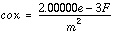
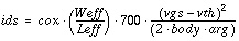
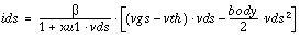
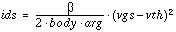
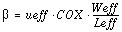
The device characteristics are modeled by process-oriented model parameters, which are mapped into model parameters at a specific bias voltage. The ids equations are as follows:
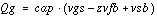
For vds < vdsat, triode region:
For vds  >=
vdsat, saturation region:
>=
vdsat, saturation region:
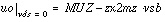
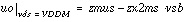
The carrier mobility, uo, is calculated by quadratic interpolation through three data points.
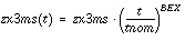
and the sensitivity of uo to vds at vds=VDDM, which is zx3ms.
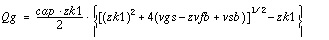
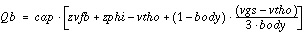
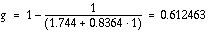
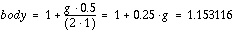
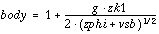
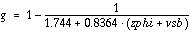
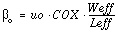
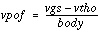
The "body" factor is calculated by:
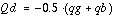
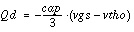
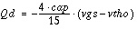
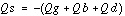
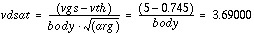
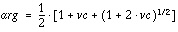
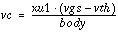
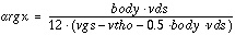
The "arg" term in saturation region current is calculated by:
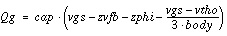
The threshold voltage can be expressed as:
The saturation voltage in the BSIM model is calculated as follows:
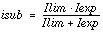
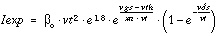
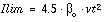
The subthreshold current isub is calculated when zn0 is less than 200 as follows:
See the Star-Hspice wire model table (resistor element) for the model parameters used.
The Star-Hspice LEVEL 13 capacitance model conserves charge and has nonreciprocal attributes. Using charge as the state variable guarantees charge conservation. You can get total stored charge in each of the gate, bulk, and channel regions by integrating the distributed charge densities/area of the active region.
The channel charge is partitioned into drain and source components in two physically significant methods by using the model parameter XPART: 40/60, or 0/100 in the saturation region, which smoothly changes to 50/50 in the triode region. XPART=0 selects 40/60 drain/source charge-partitioning in the saturation region, while XPART=1 and XPART=0.5 select 0/100 and 50/50 for drain/source charge-partitioning in the saturation region, respectively.
Star-Hspice internally protects against conditions in the LEVEL 13 model that would cause convergence problems due to negative output conductance. The constraints imposed are:
These constraints are imposed after length and width adjustment and
1. Devices exhibit self-heating during characterization, which causes declining I
2. The extraction technique produces parameters that result in negative conductance.
3. Voltage simulation is attempted outside the characterized range of the device.
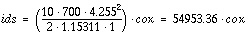
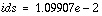
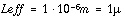
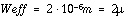
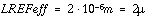
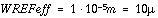
To verify the equations, it is helpful to do very simple tests using Star-Hspice and check the results with a hand calculator. Check threshold, vdsat, and ids for a very simple model, with many parameters set to zero. There is no series resistance, RSH=0. Diode current has been turned off, JS=JSW=IS=0. The LEVEL 13 subthreshold current has been turned off by n0=200. The geometry parameters are set to zero, so Leff=L=1u, Weff=W=1u.
A value of TOX has been chosen to give:
The test is at vbs=-0.35, so that phi-vbs=1.0:
.print ids=lx4(m1) vth=lv9(m1) vdsat=lv10(m1)
+ acm=2 rsh=0 js=0 jsw=0 is=0 n0=200
1.09907e-02 7.45000e-01 3.69000e+00
At vds=VDDM (default VDDM=5), mobility=mus=700
These calculations agree with the Star-Hspice results given above.
The following names are HSPICE-specific: U00, DL0, DW0, PHI0, ETA0, NB0, ND0. A zero was added to the SPICE names to avoid conflicts with other standard Star-Hspice names. For example, U0 cannot be used because it is an alias for UB, the mobility parameter in many other levels. DL cannot be used because it is an alias for XL, a geometry parameter available in all levels.
Star-Hspice supports the use of DL0 and DW0, but the use of XL, LD, XW, WD is recommended instead (noting the difference in units).
Watch the units of TOX. It is safest to enter a number greater than one, which is always interpreted as Angstroms.
1. Set X3U1, LX3U1 and WX3U1 to zero.
zx3ms>=0, where zx3ms=X3MS, with L, W adjustment
A cross-reference table for UCB's BSIM1 and Avant!'s LEVEL 13 model parameters is provided for comparison. Units are given in brackets. The Star-Hspice parameter name is given only if it differs from the SPICE name. The model specifies units for Star-Hspice parameters only if they differ from SPICE's. Star-Hspice aliases are in parentheses. Note that some Star-Hspice aliases match the SPICE names.
An asterisk (*) in front of a UCB SPICE name denotes an incompatibility between the Star-Hspice name and the UCB SPICE name (that is, the Star-Hspice alias does not match, or units are different).
Even when there is a difference in parameter name between Star-Hspice and SPICE, the corresponding L and W sensitivity parameter names might not differ. L and W sensitivity parameters are only listed for the few cases for which there is a difference.
In UCB SPICE, you must specify all BSIM model parameters. In Star-Hspice, there are defaults for the parameters.
ACM > 0 invokes Star-Hspice parasitic diodes. ACM=0 (default) is SPICE style.
The model reference temperature TNOM's default is 25°C in Star-Hspice unless .OPTION SPICE is set, causing TNOM to default to 27°C. This option also sets some other SPICE compatibility parameters. Star-Hspice TNOM is set in an .OPTION line in the netlist and can always be overridden locally (that is, for a model) with model parameter TREF. (The model "reference temperature" means that the model parameters were extracted at and are valid at that temperature).
In UCB SPICE, TNOM (default 27°C) is not effective for BSIM, and the model parameter TEMP is used instead (and must be specified) as both the model reference temperature and analysis temperature. The analysis at TEMP only applies to thermally activated exponentials in the model equations. There is no adjustment of model parameter values with TEMP. It is assumed that the model parameters were extracted at TEMP, TEMP being both the reference and the analysis temperature.
In contrast to UCB SPICE's BSIM, Star-Hspice LEVEL 13 does provide for temperature analysis. The default analysis temperature is 25°C in Star-Hspice (and 27°C in UCB SPICE for all model levels except for BSIM, as explained in the previous paragraph). Use a .TEMP statement in the Star-Hspice netlist to change the Star-Hspice analysis temperature.
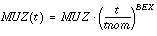
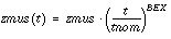
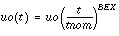
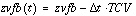
Star-Hspice provides two temperature coefficients for the LEVEL 13 model, TCV and BEX. Threshold voltage is adjusted by
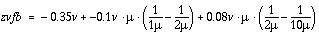
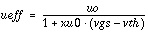
There are two implementations of the BEX factor, selected by the UPDATE parameter, which is described in the next section. The mobility in BSIM is a combination of five quantities: MUZ, zmus, z3ms, zx2mz, and zx2ms.
Note: This is equivalent to multiplying the final mobility by thefactor.
The UPDATE parameter selects between variations of the BSIM equations. UPDATE=0 is the default, which is consistent with UCB SPICE3. UPDATE=3 also is consistent with UCB SPICE3 and BEX usage.
Here is the sequence of UPDATE choices, which were responses to specific customer requests.
The special X2E equation, for UPDATE=1 only, is
The special X2E equation was requested to match a parameter extraction program. Whenever you use a parameter extraction program, the equations should be checked carefully.
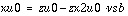
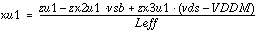
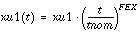
The original U1 equation divides by Leff in microns,
This is one of the few places where Leff enters explicitly into the BSIM equations; usually the Leff variation is handled by the L-adjustment model parameters, such as LU1. Physically xu1 should decrease as 1/Leff at long channels, but when dealing with short-channel devices, you can turn off this variation. Set UPDATE=2 to remove the 1/Leff factor in the xu1 equation.
UPDATE=2 introduces the present BEX usage as the 1/Leff removal ability. UPDATE=3 provides the present BEX usage with the previous xu1 equation.
FILE:ML13IV.SP IDS AND VGS CURVES FOR PMOS AND NMOS
.DC VDDN 0 5.0 .1 VBBN 0 -3 -3
*N-CHANNEL I D S CURVES (VD=0 to 5, VG=1,2,3,4,5, VB=0,-3)
.PRINT DC I(VN1) I(VN2) I(VN3) I(VN4) I(VN5) V(90)
.PLOT DC I(VN1) I(VN2) I(VN3) I(VN4) I(VN5)
*P-CHANNEL I D S CURVES (VD=0 to -5,VG=-1,-2,-3,-4,-5,VB=0,3)
.PRINT DC I(VP1) I(VP2) I(VP3) I(VP4) I(VP5) V(90)
.PLOT DC I(VP1) I(VP2) I(VP3) I(VP4) I(VP5)
* N-CHANNEL LX7=GM (VD=5, VG=0 to ->5, VS=0, VB=0,-3)
* N-CHANNEL LX8=GD (VD=0 to 5,VG=5, VS=0, VB=0,-3)
* N-CHANNEL LX9=GB (VD=5, VG=5, VS=0, VB=0 to -5)
.PLOT DC LX7(M21) LX8(M5) LX9(M31)
* P-CHANNEL LX7=GM (VD=0, VG=0->-5, VS=-5 VB=0,3)
* P-CHANNEL LX8=GD (VD=0 to -5,VG=-5, VS=-5, VB=0,3)
* P-CHANNEL LX9=GB (VD=0, VG=0, VS=-5, VB=0- >5)
.PLOT DC LX7(M22) LX8(M15) LX9(M32)
* Preliminary MOSIS BSIM parameters for SPICE3:
* The following parameters were extracted from a MOSIS
* experimental 1.2 um fabrication run.
.MODEL PC_NM1 NMOS LEVEL=13 VFB0=
+-8.27348E-01, 1.42207E-01, 3.48523E-02
+ 7.87811E-01, 0.00000E+00, 0.00000E+00
+ 9.01356E-01,-1.96192E-01, 1.89222E-02
+ 4.83095E-02,-4.10812E-02,-2.21153E-02
+ 2.11768E-03, 3.04656E-04,-1.14155E-03
+ 4.93528E+02, 5.39503E-02, 4.54432E-01
+ 5.81155E-02, 4.95498E-02,-1.96838E-02
+-5.88405E-02, 6.06713E-01, 4.88790E-03
+ 9.22649E+00,-8.66150E+00, 9.55036E+00
+-7.95688E-04, 2.67366E-03, 3.88974E-03
+ 2.14262E-03,-7.19261E-04,-3.56119E-03
+ 2.05529E-03,-3.66841E-03, 1.86866E-03
+-1.64733E-02,-3.63561E-03, 3.59209E-02
+ 4.84793E+02, 3.14763E+02,-3.91874E+01
+-4.21265E+00,-7.97847E+00, 3.50692E+01
+-5.83990E+00, 6.64867E+01,-1.99620E+00
+-1.44106E-02, 8.14508E-02, 7.56591E-04
+ 2.30000E-02, 2.30000E+01, 5.00000E+00
+ 5.04000E-10, 5.04000E-10, 1.91000E-09
+ 1.00000E+00, 0.00000E+00, 0.00000E+00
+ 2.00000E+02, 0.00000E+00, 0.00000E+00
+ 0.00000E+00, 0.00000E+00, 0.00000E+00
+ 0.00000E+00, 0.00000E+00, 0.00000E+00
+80.0,7.000E-004,4.20E-010,1.00E-008,0.700E000
.MODEL PC_PM1 PMOS LEVEL=13 VFB0=
+-5.63441E-01,-1.06809E-01, 1.32967E-01
+ 7.46390E-01, 0.00000E+00, 0.00000E+00
+ 6.57533E-01, 1.94464E-01,-1.60925E-01
+-2.55036E-03, 1.14752E-01,-8.78447E-02
+-5.59772E-03, 2.50199E-02,-5.66587E-04
+ 1.73854E+02, 2.72457E-01, 6.57818E-01
+ 1.26943E-01, 4.25293E-02,-4.31672E-02
+-1.00718E-02, 1.50900E-01,-1.00228E-02
+ 1.03128E+01,-3.94500E+00, 1.87986E+00
+ 1.55874E-03, 4.80364E-03,-1.45355E-03
+ 4.20214E-04,-2.05447E-03,-7.44369E-04
+ 1.00044E-02,-4.43607E-03, 1.05796E-03
+-5.64102E-04, 1.97407E-03, 6.65336E-04
+ 1.77550E+02, 1.02937E+02,-2.94207E+01
+ 8.73183E+00, 1.51499E+00, 9.06178E-01
+ 1.11851E+00, 9.75265E+00,-1.88238E+00
+-4.70098E-05, 9.43069E-04,-9.19946E-05
+ 2.30000E-02, 2.30000E+01, 5.00000E+00
+ 1.00000E-09, 1.00000E-09, 1.91000E-09
+ 1.00000E+00, 0.00000E+00, 0.00000E+00
+ 2.00000E+02, 0.00000E+00, 0.00000E+00
+ 0.00000E+00, 0.00000E+00, 0.00000E+00
+ 0.00000E+00, 0.00000E+00, 0.00000E+00
+140.0,4.0E-004,2.4E-010,1.00E-008,0.700E000
*NOT REFERENCED BY ANY ELEMENTS IN THIS CIRCUIT,
+ VFB0=-8.27348E-01 LVFB=1.42207E-01 WVFB=3.48523E-02
+ PHI0=7.87811E-01 LPHI=0.00000E+00 WPHI=0.00000E+00
+ K1=9.01356E-01 LK1=-1.96192E-01 WK1=1.89222E-02
+ K2=4.83095E-02 LK2=-4.10812E-02 WK2=-2.21153E-02
+ ETA0=2.11768E-03 LETA=3.04656E-04 WETA=-1.14155E-03
+ MUZ=4.93528E+02 DL0=5.39503E-02 DW0=4.54432E-01
+ U00=5.81155E-02 LU0=4.95498E-02 WU0=-1.96838E-02
+ U1=-5.88405E-02 LU1=6.06713E-01 WU1=4.88790E-03
+ X2M=9.22649E+00 LX2M=-8.66150E+00 WX2M=9.55036E+00
+ X2E=-7.95688E-04 LX2E=2.67366E-03 WX2E=3.88974E-03
+ X3E=2.14262E-03 LX3E=-7.19261E-04 WX3E=-3.56119E-03
+ X2U0=2.05529E-03 LX2U0=-3.66841E-03 WX2U0=1.86866E-03
+ X2U1=-1.64733E-02 LX2U1=-3.63561E-03 WX2U1=3.59209E-02
+ MUS=4.84793E+02 LMS=3.14763E+02 WMS=-3.91874E+01
+ X2MS=-4.21265E+00 LX2MS=-7.97847E+00 WX2MS=3.50692E+01
+ X3MS=-5.83990E+00 LX3MS=6.64867E+01 WX3MS=-1.99620E+00
+ X3U1=-1.44106E-02 LX3U1=8.14508E-02 WX3U1=7.56591E-04
+ TOXM=2.30000E-02 TEMPM=2.30000E+01 VDDM=5.00000E+00
+ CGDOM=5.04000E-10 CGSOM=5.04000E-10 CGBOM=1.91000E-09
+ XPART=1.00000E+00 DUM1=0.00000E+00 DUM2=0.00000E+00
+ N0=2.00000E+02 LN0=0.00000E+00 WN0=0.00000E+00
+ NB0=0.00000E+00 LNB=0.00000E+00 WNB=0.00000E+00
+ ND0=0.00000E+00 LND=0.00000E+00 WND=0.00000E+00
+ RSHM=80.0 CJM=7.000E-004 CJW=4.20E-010
+ IJS=1.00E-008 PJ=0.700E000
+ PJW=0.8000E000 MJ0=0.5 MJW=0.33
+ WDF=0 DS=0
.MODEL PC_PM1 PMOS LEVEL=13
+ VFB0=-5.63441E-01 LVFB=-1.06809E-01 WVFB=1.32967E-01
+ PHI0=7.46390E-01 LPHI=0.00000E+00 WPHI=0.00000E+00
+ K1=6.57533E-01 LK1=1.94464E-01 WK1=-1.60925E-01
+ K2=-2.55036E-03 LK2=1.14752E-01 WK2=-8.78447E-02
+ ETA0=-5.59772E-03 LETA=2.50199E-02 WETA=-5.66587E-04
+ MUZ=1.73854E+02 DL0=2.72457E-01 DW0=6.57818E-01
+ U00=1.26943E-01 LU0=4.25293E-02 WU0=-4.31672E-02
+ U1=-1.00718E-02 LU1=1.50900E-01 WU1=-1.00228E-02
+ X2M=1.03128E+01 LX2M=-3.94500E+00 WX2M=1.87986E+00
+ X2E=1.55874E-03 LX2E=4.80364E-03 WX2E=-1.45355E-03
+ X3E=4.20214E-04 LX3E=-2.05447E-03 WX3E=-7.44369E-04
+ X2U0=1.00044E-02 LX2U0=-4.43607E-03 WX2U0=1.05796E-03
+ X2U1=-5.64102E-04 LX2U1=1.97407E-03 WX2U1=6.65336E-04
+ MUS=1.77550E+02 LMS=1.02937E+02 WMS=-2.94207E+01
+ X2MS=8.73183E+00 LX2MS=1.51499E+00 WX2MS=9.06178E-01
+ X3MS=1.11851E+00 LX3MS=9.75265E+00 WX3MS=-1.88238E+00
+ X3U1=-4.70098E-05 LX3U1=9.43069E-04 WX3U1=-9.19946E-05
+ TOXM=2.30000E-02 TEMPM=2.30000E+01 VDDM=5.00000E+00
+ CGDOM=1.00000E-09 CGSOM=1.00000E-09 CGBOM=1.91000E-09
+ XPART=1.00000E+00 DUM1=0.00000E+00 DUM2=0.00000E+00
+ N0=2.00000E+02 LN0=0.00000E+00 WN0=0.00000E+00
+ NB0=0.00000E+00 LNB=0.00000E+00 WNB=0.00000E+00
+ ND0=0.00000E+00 LND=0.00000E+00 WND=0.00000E+00
*p+ diffusion layer
+ RSHM=140.0 CJM=4.0E-004 CJW=2.4E-010
+ IJS=1.00E-008 PJ=0.700E000
+ PJW=0.8000E000 MJ0=0.5 MJW=0.33
+ WDF=0 DS=0
*NOT REFERENCED BY ANY ELEMENTS IN THIS CIRCUIT,
Star-Hspice Manual - Release 2001.2 - June 2001


 (see subthreshold current)
 ,
UPDATE=2
,
UPDATE=2
 , UPDATE=0, 1


 , UPDATE=0, 2
 , UPDATE=1
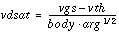


 UPDATE=0, 1
 UPDATE=0, 1
 UPDATE=2


 then,
then,

 then,
then,