You can use capacitance model parameters with all MOSFET model statements.
Model charge storage using fixed and nonlinear gate capacitances and junction capacitances. Gate-to-drain, gate-to-source, and gate-to-bulk overlap capacitances are represented by three fixed-capacitance parameters: CGDO, CGSO, and CGBO. The algorithm used for calculating nonlinear, voltage-dependent MOS gate capacitance depends on the value of model parameter CAPOP.
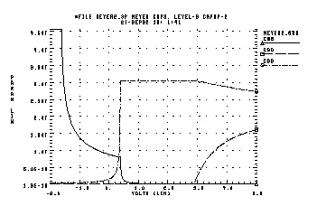
Model MOS gate capacitances, as a nonlinear function of terminal voltages, using Meyer's piecewise linear model for all MOS levels. The charge conservation model is also available for MOSFET model LEVELs 2 through 7, 13, and 27. For LEVEL 1, the model parameter TOX must be specified to invoke the Meyer model. The Meyer, Modified Meyer, and Charge Conservation MOS Gate Capacitance models are described in detail in the following subsections.
Some of the charge conserving models (Ward-Dutton or BSIM) can cause "timestep too small" errors when no other nodal capacitances are present.
Gate capacitance model selection has been expanded to allow various combinations of capacitor models and DC models. Older DC models can now be incrementally updated with the new capacitance equations without having to move to a new DC model. You can select the gate capacitance with the CAPOP model parameter to validate the effects of different capacitance models.
The capacitance model selection parameter CAPOP is associated with the MOS models. Depending on the value of CAPOP, different capacitor models are used to model the MOS gate capacitance: the gate-to-drain capacitance, the gate-to- source capacitance, or the gate-to-bulk capacitance. CAPOP allows for the selection of several versions of the Meyer and charge conservation model.
Some of the capacitor models are tied to specific DC models (DC model level in parentheses below). Other models are designated as general and can be used by any DC model.
|
Parameterized Modified Meyer model with Simpson integration (general) |
|
|
Charge conservation model (analytic), LEVELs 2, 3, 6, 7, 13, 28, and 39 only |
|
CAPOP=4 selects the recommended charge-conserving model from among CAPOP=11, 12, or 13 for the given DC model.
The proprietary models, LEVEL 5, 17, 21, 22, 25, 31, 33, and the SOS model LEVEL 27 have their own built-in capacitance routines.
If you have a capacitor with two terminals, 1 and 2 with charges Q1 and Q2 on the two terminals that sum to zero, for example, Q1=-Q2, the charge is a function of the voltage difference between the terminals, V12=V1-V2. The small-signal characteristics of the device are completely described by one quantity, C=dQ1/dV12.
If you have a four-terminal capacitor, the charges on the four terminals must sum to zero (Q1+Q2+Q3+Q4=0), and they can only depend on voltage differences, but they are otherwise arbitrary functions. So there are three independent charges, Q1, Q2, Q3, that are functions of three independent voltages V14, V24, V34. Hence there are nine derivatives needed to describe the small-signal characteristics.
It is convenient to consider the four charges separately as functions of the four terminal voltages, Q1(V1,V2,V3,V4), ... Q4(V1,V2,V3,V4). The derivatives form a four by four matrix, dQi/dVj, i=1,.4, j=1,.4. This matrix has a direct interpretation in terms of AC measurements. If an AC voltage signal is applied to terminal j with the other terminals AC grounded, and AC current into terminal i is measured, the current is the imaginary constant times 2*pi*frequency times dQi/dVj.
The fact that the charges sum to zero requires each column of this matrix to sum to zero, while the fact that the charges can only depend on voltage differences requires each row to sum to zero.
In general, the matrix is not symmetrical:
dQi/dVj need not equal dQj/dVi
This is not an expected event because it does not occur for the two terminal case. For two terminals, the constraint that rows and columns sum to zero.
forces dQ1/dV2 = dQ2/dV1. For three or more terminals, this relation does not hold in general.
The terminal input capacitances are the diagonal matrix entries
and the transcapacitances are the negative of off-diagonal entries
Cij = -dQi/dVj i not equal to j
All of the Cs are normally positive.

In MOS Capacitances, Cij determines the current transferred out of node i from a voltage change on node j. The arrows, representing direction of influence, point from node j to node i.
A MOS device with terminals D G S B provides:
CGG represents input capacitance: a change in gate voltage requires a current equal to CGGxdVG/dt into the gate terminal.
CGD represents Miller feedback: a change in drain voltage gives a current equal to CGGxdVG/dt out of the gate terminal.
CDG represents Miller feedthrough, capacitive current out of the drain due to a change in gate voltage.
To see how CGD might not be equal to CDG, the following example presents a simplified model with no bulk charge, with gate charge a function of VGS only, and 50/50 partition of channel charge into QS and QD:
Therefore, in this model there is Miller feedthrough, but no feedback.
Six capacitances are reported in the operating point printout:
These capacitances include gate-drain, gate-source, and gate-bulk overlap capacitance, and drain-bulk and source-bulk diode capacitance. Drain and source refer to node 1 and 3 of the MOS element, that is, physical instead of electrical.
For the Meyer models, where the charges like QD are not well defined, the printout quantities are:
The MOS element template printouts for gate capacitance are LX18 - LX23 and LX32 - LX34. From these nine capacitances the complete four-by-four matrix of transcapacitances can be constructed. The nine LX printouts are:
These capacitances include gate-drain, gate-source, and gate-bulk overlap capacitance, and drain-bulk and source-bulk diode capacitance. Drain and source refer to node 1 and 3 of the MOS element, that is, physical instead of electrical.
For an NMOS device with source and bulk grounded, LX18 represents the input capacitance, LX33 the output capacitance, -LX19 the Miller feedback capacitance (gate current induced by voltage signal on the drain), and -LX32 represents the Miller feedthrough capacitance (drain current induced by voltage signal on the gate).
A device operating with node 3 as electrical drain, for example an NMOS device with node 3 at higher voltage than node 1, is said to be in reverse mode. The LXs are physical, but you can translate them into electrical definitions by interchanging D and S:
CDD(reverse) = CSS = dQS/dVS = d(-QG-QB-QD)/dVS = -LX20-LX23-LX34
CDG(reverse) = CSG = -dQS/dVG = d(QG+QB+QD)/dVG = LX18+LX21+LX32
For the Meyer models, the charges QD, and so forth, are not well defined. The formulas such as LX18= CGG, LX19= -CGD are still true, but the transcapacitances are symmetrical; for example, CGD=CDG. In terms of the six independent Meyer capacitances, cgd, cgs, cgb, cdb, csb, cds, the LX printouts are:
The following example shows a gate capacitance calculation in detail for a BSIM model. TOX is chosen so that:
Vfb0, phi, k1 are chosen so that vth=1v. The AC sweep is chosen so that  for the last point.
m d g 0 b nch l=0.8u w=100u ad=200e-12 as=200e-12
.print CGG=lx18(m) CDD=lx33(m) CGD=par(`-lx19(m)')
+ CDG=par(`-lx32(m)')
.print ig_imag=ii2(m) id_imag=ii1(m)
.model nch nmos level=13 update=2
+ xqc=0.6 toxm=345.315 vfb0=-1 phi0=1 k1=1.0 muz=600
+ mus=650 acm=2
+ xl=0 ld=0.1u meto=0.1u cj=0.5e-4 mj=0 cjsw=0
BSIM equations for internal capacitance in saturation with xqc=0.4:
15.91550k 84.6886f 30.0000f 20.0000f 35.9999f
159.15500k 84.6886f 30.0000f 20.0000f 35.9999f
The calculation and the Star-Hspice results match.
The following input file shows how to plot gate capacitances as a function of bias. Set the .OPTION DCCAP to turn on capacitance calculations for a DC sweep. The model used is the same as for the previous calculations.
m d g 0 b nch l=0.8u w=100u ad=200e-12 as=200e-12
+ CGD=par(`-lx19(m)') CDG=par(`-lx32(m)')
+ CGS=par(`-lx20(m)') CSG=par(`lx18(m)+lx21(m)+lx32(m)')
+ CGB=par(`lx18(m)+lx19(m)+lx20(m)') CBG=par(`-lx21(m)')
+ level=13 update=2 xqc=0.6 toxm=345.315
+ vfb0=-1 phi0=1 k1=1.0 muz=600 mus=650
+ acm=2 xl=0 ld=0.1u meto=0.1u

The control options affecting the CAPOP models are SCALM, CVTOL, DCSTEP, and DCCAP. SCALM scales the model parameters, CVTOL controls the error tolerance for convergence for the CAPOP=3 model (see Defining CAPOP=3 -- Gate Capacitances (Simpson Integration)). DCSTEP models capacitances with a conductance during DC analysis. DCCAP invokes calculation of capacitances in DC analysis.
The parameters scaled by the option SCALM are CGBO, CGDO, CGSO, COX, LD, and WD. SCALM scales these parameters according to fixed rules that are a function of the parameter's units. When the model parameter's units are in meters, the parameter is multiplied by SCALM. For example, the parameter LD has units in meters, its scaled value is obtained by multiplying the value of LD by SCALM. When the units are in meters squared, the parameter is multiplied by SCALM
|
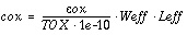
Oxide capacitance. If COX is not input, it is calculated from TOX. The default value corresponds to the TOX default of 1e-7: |
|||
|
Represents the oxide thickness, calculated from COX when COX is input. The program uses default if COX is not specified. For TOX>1, unit is assumed to be Angstroms. But a level-dependent default can override it. See specific level in Selecting MOSFET Models: LEVEL 1-40 |
|
Coefficient of channel charge share attributed to drain; its range is 0.0 to 0.5. This parameter applies only to CAPOP=4 and some of its level-dependent aliases. |
Parameter rules for gate capacitance charge sharing coefficient, XQC & XPART, in the saturation region:
The only difference is the treatment of the parameter value 0.
After XPART/XQC is specified, the gate capacitance is ramped from 50/50 at Vds=0 volt (linear region) to the value (with Vds sweep) in the saturation region specified by XPART/XQC. This charge sharing coefficient ramping ensures the smoothness of the gate capacitance characteristic.
The overlap capacitors are common to all models. You can input them explicitly, or the program calculates them. These overlap capacitors are added into the respective voltage-variable capacitors before integration and the DC operating point reports the combined parallel capacitance.
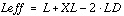
The Leff is calculated for each model differently, and it is given in the corresponding model section. The Weff calculation is not quite the same as weff given in the model LEVEL 1, 2, 3, 6, 7 and 13 sections.
The 2·WDscaled factor is not subtracted.
Strong Inversion Saturation Region, vgs > vth and vds >= vdsat
Strong Inversion Linear Region, vgs > vth and vds < vdsat
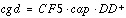
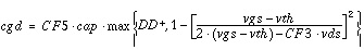
The gate-drain capacitance has value only in the linear region.
Strong Inversion Linear Region, vgs > vth and vds < vdsat.
*file capop0.sp---capop=0 capacitances
*this file is used to create spice meyer gate c-v plots
*(capop=0) for low vds and high vds
.options acct=2 post=2 dccap=1 nomod
.print dc cgb_vdsp05=par(`-lx21(m1)')
+ cgd_vdsp05=par(`-lx19(m1)') cgs_vdsp05=par(`-lx20(m1)')
.print dc cgb_vdsp8=par(`-lx21(m2)') cgd_vdsp8=par(`-lx19(m2)')
*******************************************
m1 d1 g1 0 0 mn l=5e-6 w=20e-6 $ create capacitances for
+ vds=0.05
m2 d2 g1 0 0 mn l=5e-6 w=20e-6 $ create capacitances for
+ vds=0.80
*******************************************
*********************************************
+ vto = 1.0 gamma = 1.40 nsub = 7.20e15
+ uo = 817 ucrit = 3.04e4 phi=.6
+ uexp = 0.102 neff = 1.74 vmax = 4.59e5
+ tox = 9.77e-8 cj = 0 cjsw = 0 js = 0

In the following equations,  ,
,  ,
,  , and
, and  are smooth factors. They are not user-defined parameters.
Accumulation, vgs <= vfb - vsb
 for model level higher than 4.
Weak Inversion, vgs < vth + 0.1
Strong Inversion, vgs >= vth + 0.1

Saturation Region, vgs < vth + vds
Linear Region, vgs >= vth + vds
Weak Inversion, vgs < vth + 0.1
Strong Inversion, vgs >= vth + 0.1

Saturation Region, vgs < vth + vds
Strong Inversion, vgs >= vth + vds
*file capop1.sp---capop1 capacitances
*this file creates the modified meyer gate c-v plots
*(capop=1) for low vds and high vds.
.options acct=2 post=2 dccap=1 nomod
.print dc cgb_vdsp05=par(`lx21(m1)')
+ cgd_vdsp05=par(`-lx19(m1)')
+ cgs_vdsp05=par(`-lx20(m1)')
.print dc cgb_vdsp8=par(`-lx21(m2)')
+ cgd_vdsp8=par(`-lx19(m2)')
*******************************************
m1 d1 g1 0 0 mn l=5e-6 w=20e-6 $creates capacitances
+ for vds=0.05
m2 d2 g1 0 0 mn l=5e-6 w=20e-6 $creates capacitances
+ for vds=0.80
*******************************************
*********************************************
+ vto = 1.0 gamma = 1.40 nsub = 7.20e15
+ tox = 9.77e-8 uo = 817 ucrit = 3.04e4
+ uexp = 0.102 neff = 1.74 vmax = 4.59e5
+ phi = 0.6 cj = 0 cjsw = 0 js = 0
The CAPOP=2 Meyer capacitance model is the more general form of Meyer capacitance. The CAPOP=1 Meyer capacitance model is the special case of CAPOP=2 when CF1=0, CF2=0.1, and CF3=1.
In the following equations,  ,
,  ,
,  , and
, and  are smooth factors. They are not user-defined parameters.
Accumulation, vgs <= vfb - vsb
 for model level higher than 4.
Depletion, vgs <= vth + CF2 - CF1
Strong Inversion, vgs > vth + max (CF2 - CF1, CF3 · vds) UPDATE=0
Strong Inversion, vgs > vth + CF2 - CF1, UPDATE=1

Weak Inversion, vgs < vth + CF2 - CF1, CF1  0
0
Saturation Region, vgs < vth + CF3 · vds
Linear Region, vgs > vth + CF3 · vds
Accumulation, vgs <= vth - CF1
Weak Inversion, vgs < vth + CF2 - CF1
Strong Inversion, vgs >= vth + CF2 - CF1
Accumulation, vgs <= vth - CF1
Saturation Region, vgs <= vth + CF3 · vds
Linear Region, vgs > vth + CF3 · vds
*file capop2.sp capop=2 capacitances
*this file creates parameterized modified gate capacitances
*(capop=2) for low and high vds.
.options acct=2 post=2 dccap=1 nomod
.print dc cgb_vdsp05=par(`-lx21(m1)')
+ cgd_vdsp05=par(`-lx19(m1)') cgs_vdsp05=par(`-lx20(m1)')
.print dc cgb_vdsp8=par(`-lx21(m2)') cgd_vdsp8=par(`-lx19(m2)')
*******************************************
m1 d1 g1 0 0 mn l=5e-6 w=20e-6 $creates capacitances for
+ vds=0.05
m2 d2 g1 0 0 mn l=5e-6 w=20e-6 $creates capacitances for
+ vds=0.80
*******************************************
*********************************************
+ vto = 1.0 gamma = 1.40 nsub = 7.20e15
+ tox = 9.77e-8 uo = 817 ucrit = 3.04e4
+ uexp = 0.102 neff = 1.74 phi = 0.6
+ vmax = 4.59e5 cj = 0 cjsw = 0 js = 0
+ capop=2 cf1=0.15 cf2=.2 cf3=.8 cf5=.666)
The CAPOP 3 model is the same set of equations and parameters as the CAPOP 2 model. The charges are obtained by Simpson numeric integration instead of the box integration found in CAPOP models 1, 2, and 6.
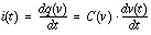
Gate capacitances are not constant values with respect to voltages. The capacitance values can best be described by the incremental capacitance:
where q(v) is the charge on the capacitor and v is the voltage across the capacitor.
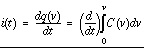
The formula for calculating the differential is difficult to derive. Furthermore, the voltage is required as the accumulated capacitance over time. The timewise formula is:
For the calculation of current:
The integral has been approximated in SPICE by:
This last formula is the trapezoidal rule for integration over two points. The charge is approximated as the average capacitance times the change in voltage. If the capacitance is nonlinear, this approximation can be in error. To estimate the charge accurately, use Simpson's numerical integration rule. This method provides charge conservation control.
To use this model, set the model parameter CAPOP to 3 and use the existing CAPOP=2 model parameters. Modify the OPTIONS settings RELV (relative voltage tolerance), RELMOS (relative current tolerance for MOSFETs), and CVTOL (capacitor voltage tolerance). The default of 0.5 is a good nominal value for CVTOL. The option CVTOL sets the number of integration steps with the formula:
Using a large value for CVTOL decreases the number of integration steps for the time interval n to n+1; this yields slightly less accurate integration results. Using a small CVTOL value increases the computational load, and in some instances, severely.
The charge conservation method (See Ward, Donald E. and Robert W. Dutton "A Charge-Oriented Model for MOS Transistor") is not implemented correctly into the SPICE2G.6 program. There are errors in the derivative of charges, especially in LEVEL 3 models. Also, channel charge partition is not continuous going from linear to saturation regions.
In Star-Hspice, these problems are corrected. By specifying model parameter CAPOP=4, the level-dependent recommended charge conservation model is selected. The ratio of channel charge partitioning between drain and source is selected by the model parameter XQC. For example, if XQC=.4 is set, then the saturation region 40% of the channel charge is associated to drain and the remaining 60% is associated to the source. In the linear region, the ratio is 50/50. In Star-Hspice, an empirical equation is used to make a smooth transition from 50/50 (linear region) to 40/60 (saturation region).
Also, the capacitance coefficients, which are the derivative of gate, bulk, drain, and source charges, are continuous. Model LEVELs 2, 3, 4, 6, 7, and 13 have a charge conservation capacitance model that is invoked by setting CAPOP=4.
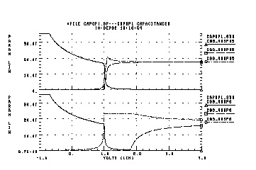
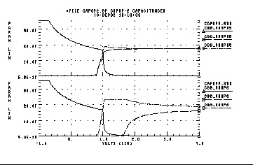
In the following example, only the charge conservation capacitance CAPOP=4 and the improved charge conservation capacitance CAPOP=9 for the model LEVEL 3 are compared. The capacitances CGS and CGD for CAPOP=4 model (SPICE2G.6) show discontinuity at the saturation and linear region boundary while the CAPOP=9 model does not have discontinuity. For the purpose of comparison, the modified Meyer capacitances (CAPOP=2) also is provided. The shape of CGS and CGD capacitances resulting from CAPOP=9 are much closer to those of CAPOP=2.
FILE MCAP3.SP CHARGE CONSERVATION MOSFET CAPS., CAPOP=4,9 LEVEL=3
* CGGB = LX18(M) DERIVATIVE OF QG WITH RESPECT TO VGB.
* CGDB = LX19(M) DERIVATIVE OF QG WITH RESPECT TO VDB.
* CGSB = LX20(M) DERIVATIVE OF QG WITH RESPECT TO VSB.
* CBGB = LX21(M) DERIVATIVE OF QB WITH RESPECT TO VGB.
* CBDB = LX22(M) DERIVATIVE OF QB WITH RESPECT TO VDB.
* CBSB = LX23(M) DERIVATIVE OF QB WITH RESPECT TO VSB.
* CDGB = LX32(M) DERIVATIVE OF QD WITH RESPECT TO VGB.
* CDDB = LX33(M) DERIVATIVE OF QD WITH RESPECT TO VDB.
* CDSB = LX34(M) DERIVATIVE OF QD WITH RESPECT TO VSB.
* THE SIX NONRECIPROCAL CAPACITANCES CGB, CBG, CGS, CSG, CGD, AND CDG
* ARE DERIVED FROM THE ABOVE CAPACITANCE FACTORS.
.print CGB=PAR(`LX18(M)+LX19(M)+LX20(M)')
+ CSG=PAR(`LX18(M)+LX21(M)+LX32(M)')
.MODEL MOS NMOS LEVEL=3 COX=1E-4 VTO=.3 CAPOP=CAPOP
+ UO=1000 GAMMA=.5 PHI=.5 XQC=XQC
+ THETA=0.06 VMAX=1.9E5 ETA=0.3 DELTA=0.05 KAPPA=0.5 XJ=.3U
+ CGSO=0 CGDO=0 CGBO=0 CJ=0 JS=0 IS=0
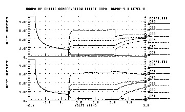
The following example tests the charge conservation capacitance model (Yang, P., B.D. Epler, and P.K. Chaterjee `An Investigation of the Charge Conservation Problem) and compares the Meyer model and charge conservation model. As the following graph illustrates, the charge conservation model gives more accurate results.
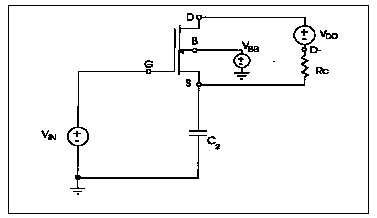
*FILE:CHRGPUMP.SP CHARGE CONSERVATION TEST FOR CHARGE PUMP CIRCUIT
*TEST CIRCUIT OF A MOSFET CAPACITOR AND A LINEAR CAPACITOR
+ RELTOL=1E-3 ABSTOL=1E-6 CHGTOL=1E-14
.TRAN 2NS 470NS SWEEP CAPOP POI 2 2,9
VIN G 0 PULSE 0 5 15NS 5NS 5NS 50NS 100NS
VBB 0 B PULSE 0 5 0NS 5NS 5NS 50NS 100NS
VDD D D- PULSE 0 5 25NS 5NS 5NS 50NS 100NS
+AD=100P AS=100P PD=50U PS=50U NRD=1 NRS=1
.MODEL MM NMOS LEVEL=3 VTO=0.7 KP=50E-6 GAMMA=0.96
+PHI=0.5763 TOX=50E-9 NSUB=1.0E16 LD=0.5E-6
+VMAX=268139 THETA=0.05 ETA=1 KAPPA=0.5 CJ=1E-4
+CJSW=0.05E-9 RSH=20 JS=1E-8 PB=0.7
.PRINT TRAN VOUT=V(S) VIN=V(D) VBB=V(B)
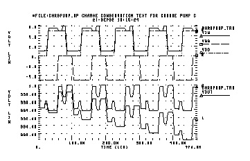
The following example applies a pulse through a constant capacitance to the gate of MOS transistor. Ideally, if the model conserves charge, the voltage at node 20 should become zero when the input pulse goes to zero. Consequently, the model that provides voltage closer to zero for node 20 conserves the charge better. As results indicate, the CAPOP=4 model is better than the CAPOP=2 model.
This example also compares the charge conservation models in SPICE2G.6 and Star-Hspice. The results indicate that Star-Hspice is more accurate.
.OPTIONS SPICE NOMOD DELMAX=.25N
.TRAN 1NS 40NS SWEEP CAPOP POI 2 4 2
VIN 1 0 PULSE (0V, 5V, 0NS, 5NS, 5NS, 5NS, 20NS)
.MODEL MOS NMOS LEVEL=2 TOX=250E-10 VTO=.3
+ UO=1000 LAMBDA=1E-3 GAMMA=.5 PHI=.5 XQC=.5
+ THETA=0.067 VMAX=1.956E5 XJ=.3U
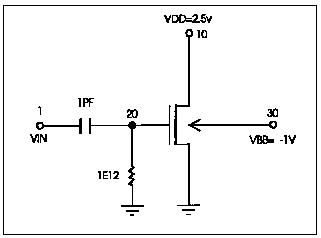
Use CAPOP=5 for no capacitors, and Star-Hspice will not calculate gate capacitance.
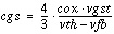
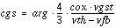
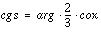
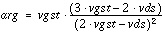
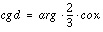
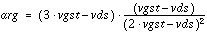
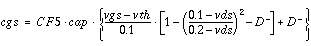
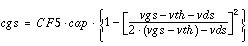
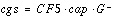
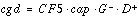
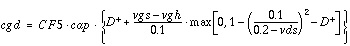
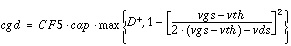
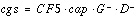
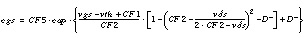
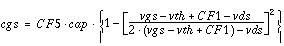
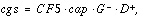
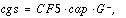
The gate capacitance cgs is calculated according to the equations below in the different regions.
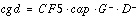
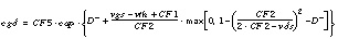
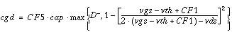
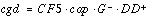
The gate capacitance cgd is calculated according to the equations below in the different regions.
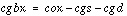
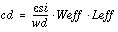
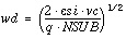
The gate capacitance cgb is combined with the calculation of both oxide capacitance and depletion capacitance as shown below.
Oxide capacitance cgbx, is calculated as:
Depletion capacitance cd is voltage-dependent.
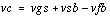
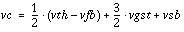
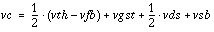
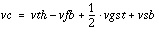
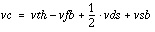
The following shows the equations for vc under various conditions:
See LEVEL 13 BSIM Model.
See LEVEL 39 BSIM2 Model.
For some MOS processes and parameter extraction methods, it is helpful to allow different Leff and Weff values for AC analysis than for DC analysis. For AC gate capacitance calculations, substitute model parameters LDAC and WDAC for LD and WD in Leff and Weff calculations. You can use LD and WD in Leff and Weff calculations for DC current.
To use LDAC and WDAC, enter XL, LD, LDAC, XW, WD, WDAC in the .MODEL statement. The model uses the following equations for DC current calculations.
and uses the following equations for AC gate capacitance calculations
The noise calculations use the DC Weff and Leff values.
Use LDAC and WDAC with the standard Star-Hspice parameters XL, LD, XW, and WD. Do not use LDAC and WDAC with other parameters such as DL0 and DW0.
Star-Hspice Manual - Release 2001.2 - June 2001


 , UPDATE=0, CF1=0
 , UPDATE=1