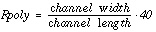
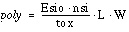
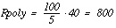
Selecting an appropriate model for I/O cell transistors improves the accuracy of simulation. For wide-channel devices, model the transistor as a group of transistors connected in parallel with appropriate RC delay networks, rather than as one transistor, because of the delay introduced by the polysilicon gate. When scaling to higher speed technologies, the area of the polysilicon gate decreases, reducing the gate capacitance. However, if you scale the gate oxide thickness, it increases the capacitance per unit area, increasing the RC product. The following example illustrates the effect on delay due to this scaling. For example, for a device with
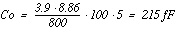
gate oxide thickness = 800 Angstroms
the resulting RC product for the polysilicon gate is
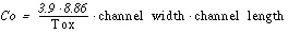
gate oxide thickness = 250 Angstroms
You can model the RC delay introduced in modern CMOS technologies by using a nine-stage ladder model.
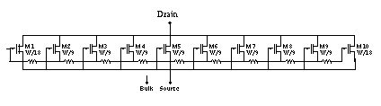
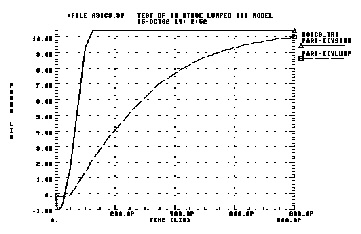
In this example, the nine-stage ladder model was entered into a Star-Hspice data file, $installdir/demo/hspice/apps /asic3.sp, and then optimized by Star-Hspice (with actual measured data of a wide channel transistor as the target data). The optimization produced a nine-stage ladder model that matched the timing characteristics of the physical data. The simulation results for the nine-stage ladder model and the one-stage model were then compared using the nine-stage ladder model as the reference. The one-stage model produces results that are about 10% faster than the actual physical data indicates.
* FILE: ASIC3.SP Test of 9 Stage Ladder Model
.subckt lrgtp drain gate source bulk
m1 drain gate source bulk p w='wt/18' l=lt
m2 drain g1 source bulk p w='wt/9' l=lt
m3 drain g2 source bulk p w='wt/9' l=lt
m4 drain g3 source bulk p w='wt/9' l=lt
m5 drain g4 source bulk p w='wt/9' l=lt
m6 drain g5 source bulk p w='wt/9' l=lt
m7 drain g6 source bulk p w='wt/9' l=lt
m8 drain g7 source bulk p w='wt/9' l=lt
m9 drain g8 source bulk p w='wt/9' l=lt
m10 drain g9 source bulk p w='wt/18' l=lt
r1 gate g1 'wt/lt*rpoly/9'
r2 g1 g2 'wt/lt*rpoly/9'
r3 g2 g3 'wt/lt*rpoly/9'
r4 g3 g4 'wt/lt*rpoly/9'
r5 g4 g5 'wt/lt*rpoly/9'
r6 g5 g6 'wt/lt*rpoly/9'
r7 g6 g7 'wt/lt*rpoly/9'
r8 g7 g8 'wt/lt*rpoly/9'
r9 g8 g9 'wt/lt*rpoly/9'
.ends lrgtp
.end pro
.end

 ,
,