LEVEL 1 IDS: Schichman-Hodges Model
This section describes the parameters and equations for the LEVEL 1 IDS: Schichman-Hodges model.
LEVEL 1 Model Parameters
The LEVEL 1 model parameters follow.
Basic Model Parameters
|
Name (Alias)
|
Units
|
Default
|
Description
|
|
LEVEL
|
|
1.0
|
DC model selector. LEVEL 1 is the Schichman-Hodges model.
|
|
COX
|
F/m
2
|
3.453e-4
|
Oxide capacitance per unit gate area. If COX is not specified, it is calculated from TOX.
|
|
KP (BET, BETA)
|
A/V2
|
|
Intrinsic transconductance parameter. If KP is not specified and UO and TOX are entered, the parameter is computed from:
KP = UO
·
COX
The default=2.0718e-5 (NMOS), 8.632e-6 (PMOS).
|
|
LAMBDA
(LAM, LA)
|
V
-1
|
0.0
|
Channel-length modulation
|
|
TOX
|
m
|
1e-7
|
Gate oxide thickness
|
|
UO
|
cm2/
(V·s)
|
|
Carrier mobility
|
Effective Width and Length Parameters
|
Name (Alias)
|
Units
|
Default
|
Description
|
|
DEL
|
m
|
0.0
|
Channel length reduction on each side.
DELscaled = DEL
·
SCALM
|
|
LD (DLAT, LATD)
|
m
|
|
Lateral diffusion into channel from source and drain diffusion.
If LD and XJ are unspecified, LD Default=0.0.
When LD is unspecified but XJ is specified, LD is calculated as: LD Default=0.75
·
XJ
LD
scaled
= LD
·
SCALM
|
|
LDAC
|
m
|
|
This parameter is the same as LD, but if LDAC is in the .MODEL statement, it replaces LD in the Leff calculation for AC gate capacitance.
|
|
LMLT
|
|
1.0
|
Length shrink factor
|
|
WD
|
m
|
0.0
|
Lateral diffusion into channel from bulk along width
WDscaled = WD
·
SCALM
|
|
WDAC
|
m
|
|
This parameter is the same as WD, but if WDAC is in the .MODEL statement, it replaces WD in the Weff calculation for AC gate capacitance.
|
|
WMLT
|
|
1.0
|
Diffusion layer and width shrink factor
|
|
XJ
|
m
|
0.0
|
Metallurgical junction depth:
XJscaled = XJ
·
SCALM
|
|
XL (DL, (LDEL)
|
m
|
0.0
|
Accounts for masking and etching effects:
XLscaled = XL
·
SCALM
|
|
XW (DW, WDEL)
|
m
|
0.0
|
Accounts for masking and etching effects:
XWscaled = XW
·
SCALM
|
Threshold Voltage Parameters
|
Name (Alias)
|
Units
|
Default
|
Description
|
|
GAMMA
|
V
1/2
|
0.5276
|
Body effect factor. If GAMMA is not specified, it is calculated from NSUB (See Common Threshold Voltage Parameters).
|
|
NFS (DFS, NF, DNF)
|
cm
-2
·
V
-1
|
0.0
|
Fast surface state density
|
|
NSUB (DNB, NB)
|
cm
-3
|
1e15
|
Bulk surface doping. NSUB is calculated from GAMMA if not specified.
|
|
PHI
|
V
|
0.576
|
Surface inversion potential -PH is calculated from NSUB if not specified (See Common Threshold Voltage Parameters).
|
|
VTO (VT)
|
V
|
|
Zero-bias threshold voltage. If not specified, it is calculated. (See Common Threshold Voltage Parameters).
|
The LEVEL 1 MOSFET model should be used when accuracy is less important than simulation turn-around time. For digital switching circuits, especially when only a "qualitative" simulation of timing and function is needed, LEVEL 1 run-time can be about half that of a simulation using the LEVEL 2 model. The agreement in timing is approximately 10%. The LEVEL 1 model, however, results in severe inaccuracies in DC transfer functions of TTL-compatible input buffers, if these buffers are present in the circuit.
The channel-length modulation parameter LAMBDA is equivalent to the inverse of the Early voltage for the bipolar transistor. LAMBDA is a measure of the output conductance in saturation. When this parameter is specified, the MOSFET has a finite but constant output conductance in saturation. If LAMBDA is not input, the LEVEL 1 model assumes zero output conductance.
LEVEL 1 Model Equations
The LEVEL 1 model equations follow.
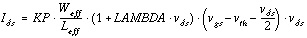
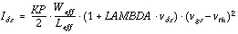
IDS Equations
In the LEVEL 1 model the carrier mobility degradation and the carrier saturation effect and weak inversion model are not included. This model determines the DC current as follows:
Cutoff Region,

Linear Region, vds < vgs - v
th
Saturation Region,  - v
th
- v
th
Effective Channel Length and Width
The model calculates the effective channel length and width from the drawn length and width as follows:


Threshold Voltage,
vth

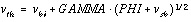
vsb < 0
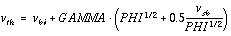
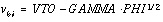
Where the built-in voltage vbi is defined as:

or
Saturation Voltage,
vsat
The saturation voltage for the LEVEL 1 model is due to channel pinch off at the drain side and is computed by:

In the LEVEL 1 model, the carrier velocity saturation effect is not included.
Star-Hspice Manual - Release 2001.2 - June 2001


